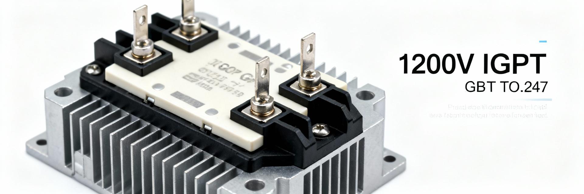
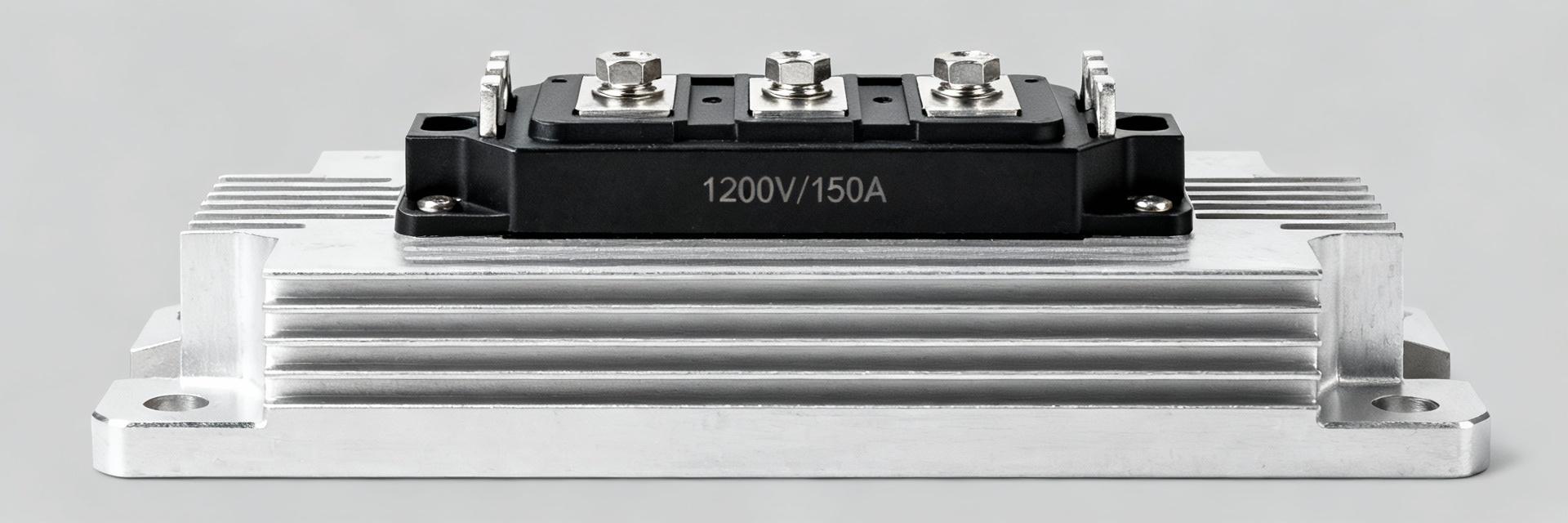
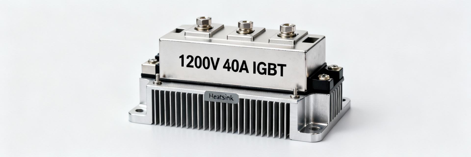
An expert analysis of the 1200V / 50A IGBT, focusing on actionable design rules for high-performance inverters and motor-drive applications.
The FGHL25T120RWD is rated for 1200 V and 50 A with a 468 W power dissipation—numbers that immediately define its suitability for high-voltage, high-current inverter and motor-drive applications. This article walks through the datasheet to extract the parameters that matter to power-design decisions: static and dynamic electrical figures, thermal limits, SOA, and practical validation steps. The goal is to turn tables and graphs into actionable design rules from the datasheet.
Readers will get concise calculation templates, a pre-layout checklist, and bench-test steps to validate designs. The guidance emphasizes how to use the datasheet to size gate drivers, cooling, and protection schemes so that the device’s headline ratings translate into reliable system performance.
Background & Part Overview
Device Classification
Point: The device is a high-voltage IGBT family member (field-stop/trench style) targeted at inverters, motor drives, and power supplies.
Evidence: Headline ratings of 1200 V, 50 A, and 468 W set the envelope for continuous conduction and switching tasks.
Explanation: In a 600–800 V DC-link inverter, the 1200 V blocking gives a safe margin; 50 A continuous current supports medium-power motors when paralleled or when thermal limits permit.
Mechanical Essentials
Point: Package and mounting drive thermal performance and layout.
Evidence: The device sits in a TO-247-style through-hole footprint with a bolted tab and large thermal pad for heatsinking.
Actionable: Confirm heatsink contact area, ensure dielectric interface (if required), reserve copper for thermal vias, and note max solder temperature before assembly.
Static & Conduction Key Specs
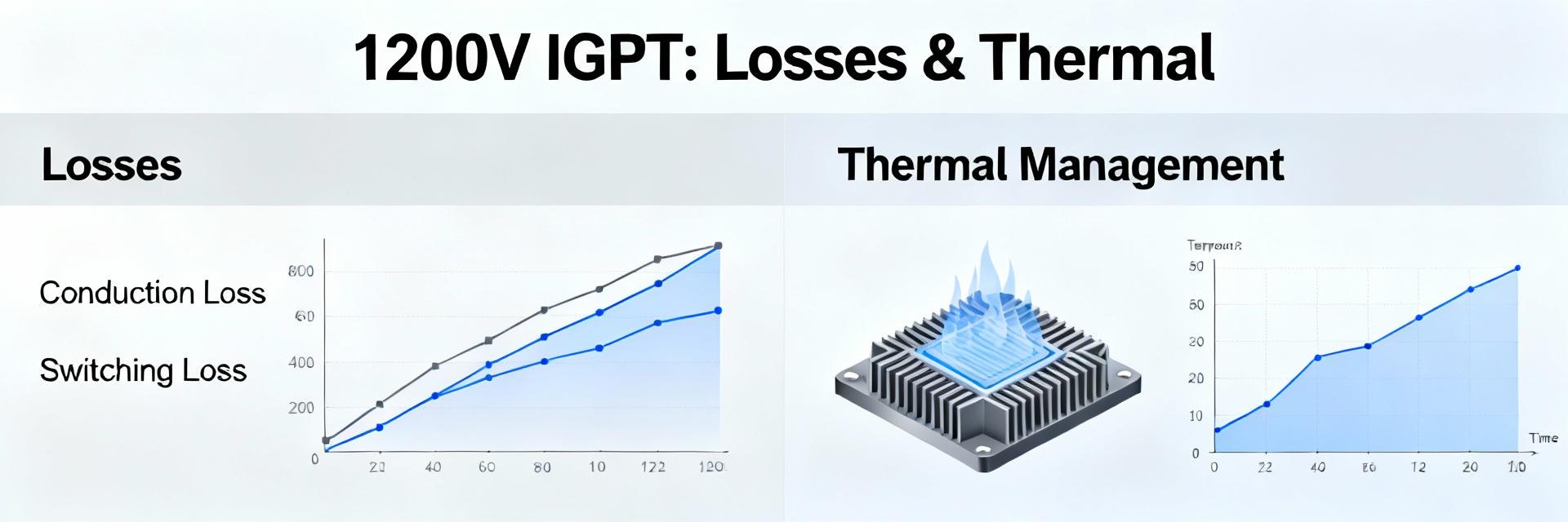
Vce(on) and Conduction Loss: Conduction loss is dominated by Vce(on) × Ic and its temperature dependence. Use Pcond = Vce(on) × Ic for steady current; include duty factor for PWM. Always use the worst-case Vce(on) at elevated junction temperature when sizing cooling systems.
Dynamic & Switching Metrics
Gate Charge & Drive Strategy
-
⚡
Peak Current: Choose a driver capable of
Idrive ≈ dVg/dt × Ciss. - ⚡ Resistor Choice: Use Rg to balance switching loss and EMI.
Switching Energy (Eon/Eoff)
Switching loss scales with frequency: Pswitch = (Eon + Eoff) × fsw. Example: Read energy at target Vce and Ic, add recovery energy, then multiply by frequency. Plotting Eswitch vs. Ic helps decide if paralleling or snubbers are necessary.
Thermal & Safe-Operating Limits
Thermal Resistance (RthJC)
Find your junction temperature rise: ΔT = Ptotal × Rth_total. If Ptotal = 60 W and desired ΔTj-case = 50 °C, required RthJC_total ≤ 0.83 °C/W. Include safety margins for high ambient temperatures.
SOA & Reliability
SOA curves and pulsed-current specs constrain overload behavior. Implement desaturation detection and fast protection to avoid exceeding SOA during turn-on faults.
Design Checklist & Application Recommendations
Pre-layout Checklist
- Extract Vce(on) vs Ic and Eon/Eoff curves.
- Note mechanical drawings for keepouts and creepage.
- Define target RthJC and heatsink requirements.
- Set gate-drive peak current demands based on Qg.
Validation Checklist
- Steady-state Vce(on) sweep across temperatures.
- Double-pulse switching tests for Eon/Eoff.
- Heatsink thermal rise with calibrated sensors.
- Controlled desaturation/short-circuit safety tests.
Key Summary
Match Vce(on) and Ic tables to calculate conduction losses and plan thermal budgets using worst-case Tj values.
Use Qg and Eon/Eoff curves to size gate driver peak current and estimate switching losses at target frequencies.
Derate blocking voltage with margin, follow SOA limits, and implement desaturation protection for fast fault clearance.
Create a one-page spec summary before layout to keep mechanical and thermal decisions aligned with datasheet numbers.

