


帮助您节省成本和时间。

为您的货物提供可靠的包装。

快速可靠的交付以节省时间。

优质的售后服务。
新品上市
更多 +


热卖零件


博客
ULV 1000 电阻器:热性能与数据汇总
核心观点: ULV 1000 电阻器的额定功率为 1000 W(安装在机箱/散热片上),而在自由空气中的能力显著降低;理解这一差异对于可靠的选型至关重要。
依据: 制造商数据表和测得的实验室运行数据一致表明,安装在散热片上与自由空气中的连续功率之间存在巨大差异。
说明: 本文汇编了测量和参考数据,以便工程师可以利用降额曲线、选择散热片,并通过可操作的图表、测试协议、安装指南和单页快速参考来验证安装。
快速洞察: 读者可以期待简洁、可测试的结果。以下章节包括测试设置、样本数据集(CSV 格式表格)、稳定标准和检查表。遵循这些协议可产生可重复的热性能结果,并为连续与间歇工作循环做出数据驱动的决策。
1 产品背景
图 1:ULV 1000 功率电阻器热分布概览
1.1 — 设计与典型结构
核心观点: 该器件是一款金属外壳绕线功率电阻器,专为机箱安装和高瞬态功耗而设计。
依据: 典型结构采用陶瓷或云母绝缘基板、绕线电阻元件和螺栓固定外壳,以便将热量传递到散热片。
说明: 结构控制着主要的热路径——元件 → 基板 → 外壳 → 散热片——因此接触面积、热界面材料和安装扭矩会显著改变给定功率下的外壳温度。ULV 1000 电阻器通常提供用于制动和负载箱范围的电阻值;选型决定了热决策。
图注: 爆炸图(元件、基板、外壳、安装支脚)——说明热路径和传感器位置。
1.2 — 额定功率与应用背景
核心观点: 额定功率取决于安装方式:正确连接到特定散热片时为 1000 W,在自由空气中则显著降低。
依据: 应用笔记显示,随着环境温度和工作循环限制的收紧,连续额定值会下降。
说明: 对于连续负载(如再生制动)使用机箱/散热片额定值,对于间歇性或通风不良的外壳则使用保守的自由空气额定值。
•典型限制: 环境温度升高、工作周期延长(>30 分钟)、气流受限、外壳辐射限制。
•设计变量: 所需连续功率、峰值脉冲功率、允许的外壳温度。
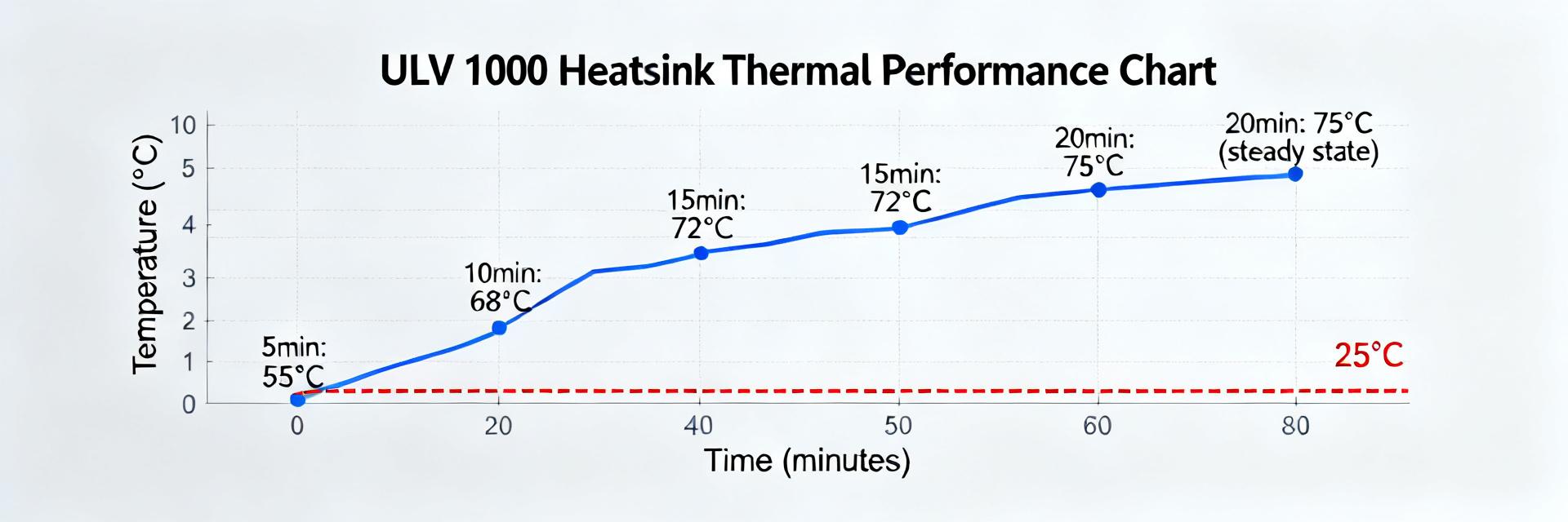
2 热性能摘要
2.1 — 需要跟踪的关键热指标
跟踪 Rθ (°C/W)、温升 (ΔT)、外壳温度、环境温度、降额曲线拐点和热时间常数。由 ΔT 除以施加功率计算出的 Rθ 给出了与环境/散热片的有效热耦合。低 Rθ 和缓慢的时间常数有利于连续散热;中等功率下的高 ΔT 信号表明需要更好的导热冷却或降低连续额定值。
2.2 — 降额曲线解读
典型的降额在环境温度阈值之前是平坦的,然后线性下降到 Tmax 时的零。实测曲线显示出稳态功率平台,随后是线性减小;瞬态脉冲在短时间内可以超过稳态限制。使用带注释的降额图表来定义安全区间:连续、允许脉冲和禁区。
3 经验数据与测试结果
功率 (W)
环境温度 (°C)
外壳温度 (°C)
温升 ΔT (°C)
热阻 Rθ (°C/W)
200
25
65
40
0.20
400
25
105
80
0.20
600
25
145
120
0.20
800
25
190
165
0.21
1000
25
240
215
0.215
4 测量协议
4.1 — 稳态热测试协议
遵循定义的顺序:预处理、增量功率(0 → 25% → 50% → 75% → 100%)、保持直至稳定(
5 安装与最佳实践
散热片选择
选择比要求更低的热阻 Rθ;确保接触面平整并控制扭矩。使用高导热率的热界面材料 (TIM),并定向散热鳍片以获得最佳气流。
常见陷阱
扭矩不足会导致温度升高 30%。没有气流的封闭机柜会导致热跳闸。如果安装脚发生变形,请务必重新加工。
6 快速参考检查表
所需连续功率 (W)、峰值脉冲功率和工作周期。
环境温度范围、允许的外壳温度和所需的散热片热阻 Rθ (°C/W)。
安装类型、TIM 规范、扭矩规范和所需的测试数据。
安全裕度: 建议连续工作时降额 ≥25%。
摘要
可靠地选择 ULV 1000 电阻器需要记录热性能、标准化测试数据以及正确的安装/冷却。在最终安装之前,运行建议的测试协议以确认设计裕度并防止热失效。
确认环境温度;根据稳态 ΔT 计算所需的散热片 Rθ。
遵循稳态协议:增量步骤、稳定(
选择 TIM 并施加受控扭矩;强迫风冷可减少降额需求。
常见问题
— ULV 1000 电阻器在连续运行时应如何降额?
仅当电阻器安装在指定的散热片上时,才应用公布的机箱/散热片额定值;对于连续运行,请从 25% 的降额裕度开始,并通过稳定测试进行验证。
— 鉴定过程中应记录哪些测试数据?
记录施加的功率、环境温度、外壳温度、ΔT、采样率和热阻 Rθ。保存原始 CSV 文件,并包含仪器校准日期以便溯源。
— 如何检测随时间推移而退化的热性能?
监测 ΔT 的趋势;ΔT 增加或热阻 Rθ 上升表示接触不良、TIM 退化或腐蚀。将定期检查结果与基准 CSV 日志进行比较。

微控制器STM32F030K6T6:一种高性能的嵌入式系统核心元器件
在当今的数字化时代,微控制器作为嵌入式系统的核心,扮演着举足轻重的角色。它们广泛应用于医疗设备、汽车电子、工业控制、消费类电子产品以及通信设备等多个领域。在这些微控制器中,STM32F030K6T6以其高性能、低功耗和丰富的外设接口等特点,成为了众多开发者心中的优选。本文将深入探讨STM32F030K6T6这一元器件的技术特点、应用领域及其在现代电子系统中的重要性。
STM32F030K6T6是由意法半导体(STMicroelectronics)推出的一款基于ARM Cortex-M0内核的微控制器,属于STM32F0系列的一员。它集成了高性能的ARM Cortex-M0 32位RISC内核,运行频率可达48MHz,提供了强大的数据处理能力。同时,该微控制器配备了高速嵌入式存储器,包括高达256KB的闪存和32KB的SRAM,足以满足大多数嵌入式应用对程序存储和数据存储的需求。
STM32F030K6T6的外设接口丰富多样,包括多个I2C、SPI和USART等通信接口,以及一个12位ADC、七个通用16位定时器和一个高级控制PWM定时器。这些外设接口为开发者提供了与外部设备通信和控制的便利,使得STM32F030K6T6能够轻松应对各种复杂的嵌入式应用场景。
低功耗是STM32F030K6T6的另一大亮点。基于ARM Cortex-M0内核的STM32F030K6T6微控制器具有较低的功耗,适用于对功耗要求严格的应用场景,如便携式设备、传感器节点等。此外,STM32F030K6T6还提供了一套全面的节能模式,允许开发者设计低功耗应用,进一步延长设备的电池寿命。
在封装方面,STM32F030K6T6提供了多种封装形式,从20引脚到64引脚不等,满足了不同应用对封装尺寸和引脚数量的需求。这种灵活性使得STM32F030K6T6能够广泛应用于各种空间受限的嵌入式系统中。
STM32F030K6T6的应用领域广泛,包括但不限于医疗设备、汽车电子、工业控制、消费类电子产品以及通信设备。在医疗设备中,STM32F030K6T6可以用于可穿戴健康监测器和便携式医疗设备中,提供精准的数据处理和可靠的通信功能。在汽车电子领域,它可用于汽车电子控制单元(ECU)、车载信息娱乐系统和车身控制系统等,提高汽车的智能化和安全性。在工业控制中,STM32F030K6T6能够控制工业自动化设备、传感器节点和机器人等,实现高效、精确的自动化生产。在消费类电子产品中,它可用于家用电器、智能家居设备和电子玩具等,提升产品的智能化和用户体验。
此外,STM32F030K6T6还得到了STMicroelectronics提供的丰富开发工具和文档支持。这些工具包括编译器、调试器、仿真器等,为开发者提供了从设计到调试的全方位支持。这些资源的存在,使得开发者能够更快速、更高效地进行项目开发,降低了开发成本和时间成本。
综上所述,STM32F030K6T6作为一款高性能的微控制器,以其强大的处理能力、丰富的外设接口、低功耗特性和灵活多样的封装形式,在嵌入式系统中发挥着举足轻重的作用。无论是医疗设备、汽车电子还是工业控制等领域,STM32F030K6T6都展现出了卓越的性能和广泛的应用前景。随着物联网和人工智能技术的不断发展,STM32F030K6T6将在未来继续引领嵌入式系统的发展潮流,为我们的生活带来更多便捷和智能。