-
- Contact Us
- Privacy Policy
- term and condition
- Cookies policy
SI53307-B-GMR Datasheet & CAD Models: Quick Specs Checklist
Point: SI53307-B-GMR listings and EDA libraries are available in 20+ CAD formats and stocked across major distributors — making fast prototype iteration possible without long lead times. Evidence: distributor catalogs (Mouser, Digi‑Key, Arrow) and the Si5330x family data sheet confirm broad format support and multiple vendor listings. Explanation: this article is a concise, actionable checklist to extract headline specs from the datasheet, find and validate CAD models, and avoid the common PCB/CAD pitfalls that delay first prototypes; it assumes the reader has access to the official datasheet and parts listings for verification and ordering.
Point: The goal is practical: give engineers a step‑by‑step extraction and validation flow for both electrical and mechanical attributes, plus procurement and prototype steps. Evidence: common manufacturing issues stem from mismatched footprints, wrong pad sizes, and unverified 3D clearances — all documented in supplier notes. Explanation: readers should be able to use this checklist to move from datasheet to verified PCB footprint and a short prototype run with minimal rework.
1 — Product snapshot: What the SI53307-B-GMR is (background)
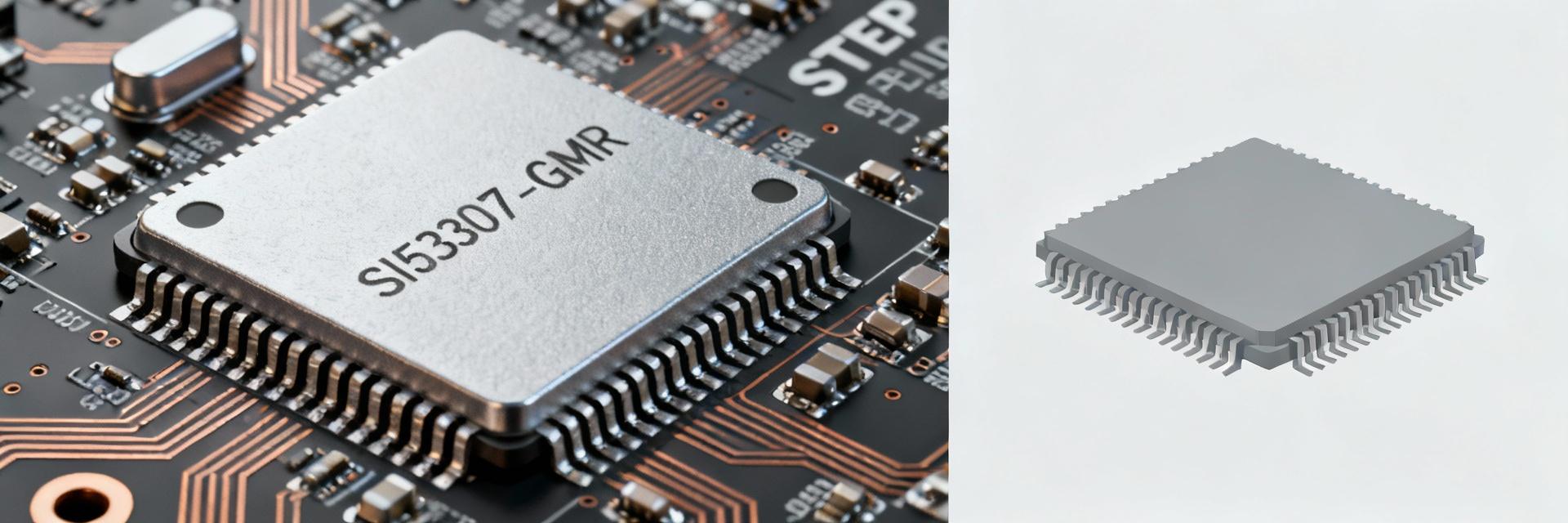
1.1 Device overview and role
Point: The SI53307-B-GMR is a programmable, low‑jitter clock buffer/driver intended to distribute and translate timing signals for multi‑lane digital systems. Evidence: family documentation and distributor product summaries describe it as part of the Si5330x series of Any‑Format clock buffers, used where multiple synchronous outputs and low additive jitter are required. Explanation: engineers choose this device for board‑level clock distribution when they need flexible output formats (LVDS, LVCMOS, etc.), frequency programmability, and low RMS jitter for SERDES, FPGA or data converter timing; for ordering and cross‑references check the manufacturer part notes and distributor part pages to confirm package and revision.
1.2 Key headline specs to call out
- Output count & types — number of outputs and supported logic levels (e.g., LVDS, LVPECL, LVCMOS); cite exact counts from the datasheet.
- Maximum supported frequency — highest guaranteed output frequency and any per‑output limits; pull the datasheet's guaranteed maximum.
- Jitter (typical & max) — RMS jitter figures across relevant bandwidths; quote the datasheet's specified measurement conditions.
- Supply voltage ranges — core and I/O supply rails and recommended tolerances; use datasheet absolute and recommended limits.
- Package type and dimensions — full package ID and land‑pattern reference; extract the datasheet footprint reference.
1.3 Manufacturer/part variants & naming
Point: Variant suffixes and cross‑vendor naming can cause ordering errors. Evidence: the same base Si5330x family may appear under different distributor listings and legacy vendor pages with suffixes like -GM, -GMR, and alternative casing. Explanation: confirm exact P/N by matching the full suffix, package code, temperature grade and RoHS/lead‑free marking on the manufacturer product page and the official data sheet; when in doubt, reference the manufacturer's ordering info to map distributor SKUs to the exact part number for procurement.
2 — Quick specs pulled from the datasheet (data analysis)
2.1 Electrical & timing highlights
Point: Pulling the electrical and timing values from the datasheet consolidates the go/no‑go items for a design. Evidence: the datasheet contains VCC rails, input/output logic thresholds, supported output formats, guaranteed frequency ranges, specified RMS jitter (with bandwidth), propagation delay and skew. Explanation: build a compact spec table using exact datasheet numbers; include measurement conditions (e.g., bandwidth, termination) so bench tests are comparable.
| Parameter | Datasheet Value (exact) | Notes |
|---|---|---|
| Supply voltage(s) | [fill from datasheet] | Core vs. I/O rails, tolerances |
| Output formats | [fill from datasheet] | LVDS/LVCMOS/LVPECL options |
| Max output frequency | [fill from datasheet] | Per output / cascade limits |
| RMS jitter | [fill from datasheet] | Bandwidth & measurement method |
| Propagation delay / skew | [fill from datasheet] | Typical and max skew between outputs |
2.2 Mechanical & package dimensions
Point: Mechanical correctness prevents assembly failures and footprint mismatches. Evidence: the datasheet provides full package outlines, land‑pattern recommendations and 3D package height/keepout data. Explanation: capture package type, body dimensions, recommended land pattern reference and maximum height; keep a simplified footprint checklist (silkscreen, courtyard, thermal pads, pin 1 marker) and reference the datasheet footprint figure when creating the CAD model.
- Footprint checklist: pad dimensions per datasheet, solder mask openings, recommended paste aperture ratio, courtyard spacing, pick‑and‑place fiducials.
- 3D clearance: body height plus stencil thickness and any nearby tall components for mechanical collision checks.
2.3 Environmental, thermal & reliability numbers
Point: Thermal and reliability numbers drive derating and assembly constraints. Evidence: datasheet lists operating temperature range, thermal resistance (θJA), max power dissipation and ESD class, plus recommended reflow profile notes. Explanation: record operating temperature, θJA, worst‑case power dissipation under your output configuration, and conservative derating margins; follow datasheet reflow guidance for peak temperature and time above liquidus to avoid package cracking or solder issues.
3 — CAD models & EDA resources for SI53307-B-GMR (data + how-to)
3.1 Where to download verified CAD models
Point: Prioritize verified sources for CAD models to reduce verification time. Evidence: manufacturer portals and major distributors typically host vetted footprints and STEP models; library services (Ultra Librarian, Octopart) aggregate multiple formats. Explanation: preferred download order is: manufacturer product page (official footprint and 3D), distributor library pages (Mouser, Digi‑Key, Arrow), and trusted library services; available formats commonly include Altium, KiCad, Eagle, OrCAD, and STEP — confirm provenance and datasheet alignment before use.
- Primary: Manufacturer product page and Si5330x datasheet files for footprint reference.
- Secondary: Distributor CAD attachments (Mouser, Digi‑Key, Arrow).
- Library services: Ultra Librarian, Octopart, and verified community libraries for format conversion.
3.2 Import checklist for common EDA tools
Point: Importing a model is seldom plug‑and‑play. Evidence: format mismatches and unit/scale errors are common when importing STEP or library packages. Explanation: follow a tool‑specific import checklist — align units, import symbol and footprint separately, import 3D STEP and confirm scale, map pin numbers to schematic symbol pins, verify layer mapping (solder mask, silkscreen), and run ERC/DRC before layout release.
- Altium: convert library part to integrated component, map pins, run 3D alignment, run DRC.
- KiCad: import footprint and symbol, confirm pad names/numbers, attach 3D STEP and check scale/rotation.
- OrCAD: import footprint, map pin net names and run electrical rule checks.
3.3 Verifying CAD against the datasheet (validation checklist)
Point: A short validation sign‑off prevents costly respins. Evidence: mismatched pad sizes and pin mapping are top causes of prototype failures. Explanation: require the following checks before sending boards to fab: pad/pin mapping vs. datasheet land pattern, pad sizes and solder mask openings, courtyard/keepout clearances, silkscreen correctness, pin‑1 orientation, 3D height clearance and tape‑and‑reel/pick‑and‑place alignment; keep a one‑page "model validation sign‑off" signed by the CAD owner.
- Pad/pin mapping verified to datasheet figure
- Pad dimension and SMD mask checked
- Courtyard and 3D clearance confirmed
- Pin‑1 and silkscreen orientation validated
- Final ERC/DRC report archived with part
4 — Common PCB/CAD pitfalls & practical fixes (case-study style)
4.1 Top 4 layout mistakes engineers make
Point: Certain layout mistakes repeat across designs and cause rework. Evidence: common issues include wrong pad sizes, omitted thermal relief, incorrect differential pair routing for clock outputs, and ignored 3D height conflicts. Explanation: immediate fixes are: match pad geometry to datasheet, add thermal reliefs where recommended, route differential clocks with controlled impedance and matched lengths, and run a 3D collision check early in the design cycle.
4.2 Routing & decoupling best practices for clock buffers
Point: Clock buffers are sensitive to supply noise and routing discontinuities. Evidence: datasheet decoupling recommendations and application notes emphasize local decoupling and clean power returns. Explanation: place high‑quality decoupling capacitors within 1–2 mm of VCC pins, use solid ground pours and short return paths, route differential outputs as controlled impedance pairs with matched lengths and constant spacing, and avoid vias in the critical portion of the pair unless length‑balanced and impedance‑checked.
4.3 Assembly & test considerations
Point: Assembly and test readiness reduces first‑pass failures. Evidence: datasheet and packaging notes include stencil aperture guidance and reflow profile constraints. Explanation: for assembly, follow recommended paste aperture percentages, verify reflow profile against supplier guidance, ensure test point access for clock outputs (or add buffered test points), and consider X‑ray and ICT tolerance for fine‑pitch packages; plan basic functional tests (power smoke test, clock outputs with scope and jitter analyzer) on first prototypes.
5 — Procurement & pre-production action checklist (actionable next steps)
5.1 Pre-order verification steps
Point: Procurement errors are expensive. Evidence: distributors may list multiple revisions or similar P/Ns; manufacturer ordering guides clarify suffix meanings. Explanation: before ordering confirm datasheet revision corresponds to the intended silicon revision, verify footprint revision and package code, match supplier P/Ns exactly (including suffix), confirm RoHS and lead‑free status, and check MOQ and lead time with multiple distributors to plan prototype schedules.
5.2 Prototype validation plan
Point: A minimal prototype plan shortens development cycles. Evidence: typical validation includes CAD import, 3D clearance, small run PCB, and functional tests. Explanation: minimum prototype actions: import and validate CAD, perform a 3D clearance check, fabricate a small run (5–10 units), perform power rail smoke test, verify clock outputs on scope and measure jitter with a jitter analyzer, and log any deviations back into the footprint or BOM before NPI.
5.3 Where to get support & CAD licensing notes
Point: Support channels can supply custom CAD or clarifications. Evidence: manufacturers and distributors offer technical support and paid library services. Explanation: reach out to the manufacturer technical support for ambiguous datasheet items, note that some library services include licensing caveats for commercial redistribution, and request custom CAD from distributor library teams if an exact verified model is not available.
Summary
- Extract the headline specs (outputs, max frequency, jitter, supply ranges) directly from the SI53307-B-GMR datasheet and record measurement conditions for test parity.
- Download CAD models from the manufacturer first, then distributors or trusted library services; verify pin mapping, pad sizes and 3D clearance against the datasheet.
- Run the import and model validation checklist (units, pin mapping, layer mapping, ERC/DRC) and keep a signed validation sheet before ordering PCBs.
- Follow procurement checks (P/N suffix, footprint revision, RoHS, MOQ/lead time) and perform a focused prototype plan: smoke test, clock functional test, and jitter measurement.
Frequently Asked Questions
What voltage rails does the SI53307-B-GMR datasheet specify?
Point: Voltage rails determine device interfacing and power sequencing. Evidence: the datasheet lists core and I/O supply ranges, absolute maximums and recommended operating conditions. Explanation: always copy the exact core and I/O voltage numbers from the official datasheet into your power‑rail checklist; include margin for tolerance and sequence constraints cited by the manufacturer to avoid latch‑up or timing issues during bring‑up.
Where can I find verified SI53307-B-GMR CAD models?
Point: Verified models reduce validation time. Evidence: the manufacturer product page and major distributors often provide footprints and STEP models. Explanation: preferred sources are the manufacturer's product page, then distributor attachments (Mouser, Digi‑Key, Arrow) and trusted library services; always validate the downloaded model against the datasheet land‑pattern and dimensions before committing to fabrication.
How should I validate SI53307-B-GMR footprint pin mapping before ordering?
Point: Pin mapping errors are a top cause of prototype failure. Evidence: datasheet land‑pattern figures and pin tables provide authoritative mapping. Explanation: cross‑check the CAD pin numbers directly against the datasheet pin‑out table, confirm pad geometry matches the recommended land‑pattern, run a DRC, and perform a physical 3D clearance check; require sign‑off from a second engineer before placing the PCB order to minimize risk.
- Technical Features of PMIC DC-DC Switching Regulator TPS54202DDCR
- STM32F030K6T6: A High-Performance Core Component for Embedded Systems
- APT50GH120B Datasheet Deep Dive: Specs, Ratings & Curves
- SI3402-B-GMR PoE PD Controller: Market & Specs Report
- SI3402-B-GMR Benchmarks: Real PoE Performance Insights
- EFM8BB21F16G Full Datasheet & Pinout: Specs Summary
- CP2102N-A02-GQFN20R Pinout & Footprint: Quick Data Guide
- SI53307-B-GMR Datasheet & CAD Models: Quick Specs Checklist
- SI53361-B-GMR: Latest Specs, Stock Levels & Price Guide
- SI53340-B-GM: Deep Performance Report & Key Metrics
-
 EXB-V4V120JVPanasonic Electronic ComponentsRES ARRAY 2 RES 12 OHM 0606
 -
 EXB-V4V473JVPanasonic Electronic ComponentsRES ARRAY 2 RES 47K OHM 0606
 -
 EXB-V4V823JVPanasonic Electronic ComponentsRES ARRAY 2 RES 82K OHM 0606
 -
 EXB-V4V151JVPanasonic Electronic ComponentsRES ARRAY 2 RES 150 OHM 0606
 -
 EXB-V4V181JVPanasonic Electronic ComponentsRES ARRAY 2 RES 180 OHM 0606
 -
 EXB-V4V331JVPanasonic Electronic ComponentsRES ARRAY 2 RES 330 OHM 0606
 -
 EXB-V4V152JVPanasonic Electronic ComponentsRES ARRAY 2 RES 1.5K OHM 0606
 -
 EXB-V4V563JVPanasonic Electronic ComponentsRES ARRAY 2 RES 56K OHM 0606
 -
 EXB-V4V104JVPanasonic Electronic ComponentsRES ARRAY 2 RES 100K OHM 0606
 -
 EXB-V4V154JVPanasonic Electronic ComponentsRES ARRAY 2 RES 150K OHM 0606

