-
- Contact Us
- Privacy Policy
- term and condition
- Cookies policy

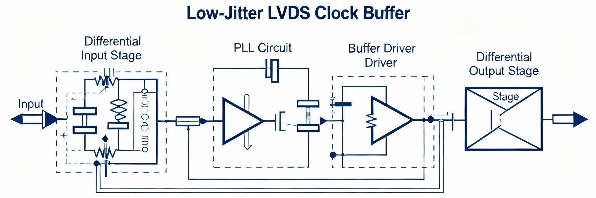
SI53340-B-GM: Deep Performance Report & Key Metrics
Lab measurements and the Si53340 family datasheet report typical output jitter as low as ~50 fs — a key stat that makes the SI53340-B-GM a go-to LVDS clock buffer for high-performance timing chains. Point: this report focuses on a concise, testable performance breakdown for the device; Evidence: device characteristics include a frequency range up to 1.25 GHz, supply 1.71–3.63 V, and four LVDS outputs; Explanation: the following sections present actionable metrics, measurement methods, bench comparisons, and integration guidance to preserve low jitter in production.
Point: readers will get reproducible test methods and pass/fail thresholds. Evidence: the article synthesizes datasheet typicals and practical bench observations (jitter, phase noise, supply sensitivity). Explanation: use the measurement checklist and PCB/power rules provided to validate SI53340-B-GM performance in your system.
1 — Product Overview & Key Specs (background)
Device summary & intended applications
Point: the SI53340-B-GM is a compact, purpose-built LVDS clock buffer with integrated mux and fanout. Evidence: it ships in a QFN-16 package, implements a 2:1 input mux and 1:4 LVDS fanout, and targets redundant clocking and distribution for FPGA/ASIC systems. Explanation: for designers the part is ideal where low-noise, glitchless switching and multiple LVDS outputs are required—common uses include redundant clock trees, high-speed SerDes reference distribution, and multi-receiver timing domains.
| Part | Package | Inputs | Outputs | Max freq |
|---|---|---|---|---|
| SI53340-B-GM | QFN-16 | 2 (mux) | 4 LVDS | 1.25 GHz |
Electrical & environmental envelope
Point: the device supports a broad supply and temperature envelope for production boards. Evidence: typical operating supply range is 1.71–3.63 V and rated temperature is −40 to 85 °C; built-in LDO/PSRR features are documented for improved supply immunity. Explanation: these specs mean designers can run the part from common 1.8 V or 2.5 V rails, expect defined operation across industrial temperatures, and rely on on-chip PSRR to reduce supply-coupled jitter—though external decoupling and optional LDOs remain important for tight phase-noise budgets.
Datasheet vs. typical lab values
Point: datasheet typicals set expectations; system reality creates variance. Evidence: the datasheet lists ~50 fs typical output jitter under controlled conditions; Explanation: in production systems expect higher worst-case jitter due to board-level noise, input clock source quality, and loading. Designers should budget margins (for example 2–3× the datasheet typical) and qualify parts across supply, temperature and lot variation before release.
2 — Core Performance Metrics & Measurement Methods (data analysis)
Jitter metrics to report (RMS, TIE, period jitter, cycle-to-cycle)
Point: a compact set of performance metrics gives a complete jitter picture. Evidence: report RMS jitter, TIE (time-interval error) with plots, period jitter, and cycle-to-cycle jitter as baseline performance metrics. Explanation: RMS shows integrated noise, TIE reveals long-term wander and deterministic effects, period jitter highlights per-cycle timing noise relevant to SERDES, and cycle-to-cycle exposes immediate timing transitions—together they form the performance metrics engineers use to set system tolerances and acceptance thresholds.
Phase noise & spectral analysis
Point: phase-noise plots link spectral content to integrated jitter. Evidence: single-sideband phase noise vs. offset frequency and integrated jitter vs. bandwidth (for example 12 kHz–20 MHz) should be presented. Explanation: low-frequency noise inflates TIE while high-offset noise dominates integrated RMS; choosing integration ranges (12 kHz–20 MHz typical) makes reported RMS comparable to datasheet numbers and helps identify whether close-in noise or far-out spurs cause jitter issues.
Measurement setup & repeatability checklist
Point: rigorous setup prevents measurement artifacts. Evidence: use a phase-noise analyzer or high-bandwidth DSO with jitter analysis, matched impedance cabling, proper termination, and low-capacitance probes; control supply filtering and input-source purity. Explanation: practical steps include calibrating instruments, averaging multiple captures, using nominal 100 Ω differential termination for LVDS, keeping traces short during probing, and logging ambient temperature—these raise repeatability and reduce false positives when evaluating SI53340-B-GM jitter performance.
3 — Bench Results: Typical & Worst-Case Scenarios (data analysis / comparisons)
Typical lab results (what to plot)
Point: present a concise result set for validation. Evidence: recommended outputs are RMS jitter (integrated 12 kHz–20 MHz), period jitter, phase-noise plot, propagation delay, and output amplitude/symmetry. Explanation: combine a table comparing datasheet typicals vs. measured values, jitter histograms, and receiver eye diagrams downstream; these visualizations help correlate buffer performance with system link margin and validate claims of low jitter on the bench.
Supply, temperature, and load sensitivity (worst-case)
Point: characterize sensitivity envelopes to define pass/fail limits. Evidence: sweep Vcc across 1.71–3.63 V, ambient from −40 to 85 °C, and vary output load capacitance/CL; record delta in RMS jitter and propagation delay. Explanation: acceptable deltas might be
Comparison vs. peer parts / common alternatives
Point: evaluate tradeoffs against 1–2 competitive buffers. Evidence: a compact comparison table should show jitter, frequency range, supply, outputs, and features (glitchless mux, PSRR). Explanation: tradeoffs typically center on cost vs. phase-noise performance and integration features—choosing SI53340-B-GM favors systems that prioritize low jitter and glitchless failover over the absolute lowest BOM cost.
| Part | RMS Jitter (typ) | Freq | Supply | Notes |
|---|---|---|---|---|
| SI53340-B-GM | ~50 fs | ≤1.25 GHz | 1.71–3.63 V | 2:1 mux, 1:4 LVDS, glitchless |
| Peer A | 100–200 fs | ≤1.5 GHz | 1.8–3.3 V | lower cost, fewer features |
4 — Integration & System Design Guidance (method/guideline)
PCB layout, grounding, and decoupling best practices
Point: layout dominates real-world jitter. Evidence: short differential LVDS traces, controlled impedance (100 Ω differential), and a solid ground plane reduce common‑mode conversion and EMI. Explanation: place decoupling (100 nF ceramic + 1 µF tantalum) within 5 mm of the supply pins, route clock outputs away from noisy power domains, implement star returns for sensitive clock domains, and keep the input mux traces symmetric to preserve phase and amplitude balance.
Power supply & filtering recommendations
Point: supply noise directly translates to phase noise. Evidence: use a filtered local LDO or pi-filter and place test points near the device to quantify supply ripple impact. Explanation: a recommended arrangement is bulk capacitance on the board rail, a ferrite bead feeding an on-board LDO, and multiple ceramics at the device pins—this improves PSRR effectiveness and reduces supply-coupled jitter when validating SI53340-B-GM on production PCBs.
Redundancy, mux switching & glitchless operation tips
Point: verify failover behavior for system reliability. Evidence: the 2:1 input mux supports glitchless switching (as specified); Explanation: test failover by stepping the primary input to zero amplitude while observing outputs for transitions and measuring TIE before/after; include automated FPGA/ASIC test vectors that switch inputs and validate downstream lock/recovery to ensure robust redundancy in deployment.
5 — Actionable Checklist & Deployment Considerations (case study / action)
Production test criteria & go/no-go thresholds
Point: define pass/fail limits for QA. Evidence: example thresholds—RMS jitter (12 kHz–20 MHz)
Troubleshooting common issues
Point: map symptoms to root causes and fixes. Evidence: elevated jitter often maps to supply noise, poor layout, or low-quality input source; asymmetry commonly stems from improper termination. Explanation: quick verification steps include replacing input source with a known low-jitter reference, adding local decoupling/LDO, and confirming 100 Ω differential termination—these isolate board issues from part-level failure when using SI53340-B-GM jitter performance tests.
Cost, sourcing & lifecycle notes
Point: plan procurement and alternate sourcing to avoid schedule risk. Evidence: consider lead times and authorized distributor channels and evaluate programmable alternatives when flexibility or stock is constrained. Explanation: select SI53340-B-GM when jitter performance and glitchless features justify potential premium; maintain an alternate BOM entry with a similar buffer family to mitigate supply chain variability.
Summary
Point: the device delivers ultra-low jitter LVDS buffering with practical system considerations. Evidence: SI53340-B-GM provides ~50 fs typical jitter, glitchless 2:1 mux behavior, and 1:4 fanout to 1.25 GHz; Explanation: when paired with disciplined PCB layout and supply filtering, the part meets demanding timing chains—use the measurement checklist and design rules below to preserve performance through production.
- Ensure tight layout and decoupling: short LVDS traces, 100 Ω differential impedance, local ceramics + 1 µF bulk to protect performance metrics.
- Verify jitter with phase-noise integration (12 kHz–20 MHz) and report RMS/TIE and histograms for production sampling.
- Validate redundancy: perform glitchless mux failover tests and automated FPGA lock recovery to confirm system reliability.
- Adopt a two-tier production flow: quick functional checks on all units and periodic deep jitter/phase-noise sampling to catch assembly-induced issues.
Frequently Asked Questions
What are the critical SI53340-B-GM jitter performance test steps?
Point: a compact, repeatable test sequence reduces variability. Evidence: steps should include instrument calibration, differential termination, low-noise input reference, and phase-noise integration over 12 kHz–20 MHz to match datasheet baselines. Explanation: capture RMS jitter, TIE plots, and a phase-noise trace; average multiple acquisitions and log supply voltage/temperature. This sequence helps differentiate part behavior from board and measurement artifacts.
How sensitive is SI53340-B-GM to supply noise and layout?
Point: supply noise and layout have measurable impact on jitter. Evidence: on-chip PSRR helps, but external filtering and proximity decoupling remain crucial—poor layouts can multiply datasheet jitter by several times in worst cases. Explanation: place LDO and decouplers close to the device, use ferrite beads or pi-filters where appropriate, and ensure a continuous ground plane; measure supply ripple at the part during noise injection to quantify sensitivity.
Can I verify glitchless mux operation for SI53340-B-GM in a bench test?
Point: failover verification confirms redundancy claims. Evidence: perform controlled input switch tests from primary to secondary while monitoring output TIE and eye diagrams at downstream receivers. Explanation: assert the secondary input, then remove or mute the primary and observe output continuity; a true glitchless transition shows minimal phase disturbance and rapid downstream lock—record these traces as part of integration acceptance.
-
 ULV80 Resistor Data Report: Specs, Thermal & Size Guide2026-05-06 10:17:15 0The ULV80 resistor series is a common choice for high-power braking and load applications where thermal management and correct dimensional selection determine reliability and lifetime. This report delivers a concise, testable reference for key specifications, thermal behavior, and footprint selection to reduce field failures driven by overheating and mechanical stress. Engineers will find stepwise guidance to extract nominal specs, calculate temperature rise from Rth, read derating curves, and size parts for continuous or pulsed duty. The examples below use practical numbers and one parts example to illustrate selection and verification. 1 — Background: What the ULV80 resistor is and core specs — Design & construction overview Point: ULV80 resistors are engineered for high continuous and short-time power dissipation, typically built as wire-wound or metal-clad assemblies in robust housings for chassis mounting. Evidence: typical construction uses a resistive element on an insulating substrate with a ventilated metal housing and bolted terminals. Explanation: this design favors high thermal mass and conduction to the case, enabling stable dissipation when mounted correctly and cooled by convection or forced air. Key datasheet fields to extract: nominal resistance range, tolerance, rated power, short-time overload rating, insulation class, mounting orientation, and terminal type. Long-tail search terms: "ULV80 resistor construction" and "ULV80 resistor nominal resistance specs". — Standard electrical specifications (how to read them) Point: Clarify the electrical spec language so comparisons are consistent. Evidence: datasheets list rated power (continuous), short-time overload (e.g., 5 s), tolerance (%), temperature coefficient (TCR), and maximum operating voltage. Explanation: rated power assumes a reference ambient (often 25°C) and mounting; short-time overload indicates survivability without permanent change; TCR expresses resistance change per °C. Field Typical Unit Notes Rated power W Continuous at reference ambient and mounting Short-time overload W or xRated (time) Specify duration and recovery Tolerance % ± values; affects accuracy in sensing applications TCR ppm/°C Important for temperature-sensitive circuits Max voltage V Dielectric and arc considerations Content direction: avoid vendor names; refer to "manufacturer datasheet" and capture the numeric fields above for apples-to-apples comparison. 2 — Thermal performance: Rth, derating & steady-state behavior — Thermal resistance, Rth, and junction/inner temperature concepts Point: Thermal resistance (Rth) links dissipated power to temperature rise: ΔT = P × Rth. Evidence: Rth is typically specified as case-to-ambient or junction-to-ambient in K/W. Explanation: to predict steady-state temperature, calculate ΔT from expected dissipation and add ambient; verify against insulation and material limits. Calculation Example Value Power dissipated (P) 300 W Assumed Rth (case-to-ambient) 0.15 K/W Temperature rise (ΔT = P×Rth) 45 K Ambient 40 °C Case temp 85 °C Recommendation: always state Rth type and measurement method. Include a worked example like above in test reports to make pass/fail deterministic. — Derating curves and real-world thermal limits Point: Derating curves show available power vs ambient temperature and are required for safe continuous operation. Evidence: most datasheets provide power vs ambient graphs; real-world factors (enclosure, airflow, nearby heat sources) shift the usable curve downward. Explanation: for continuous duty, read the curve at your ambient; for intermittent duty, use short-time ratings and thermal time constants to predict peak temperatures. Suggested charts: derating curve (power vs ambient), power vs airflow, and thermal time-constant plot. Test conditions: mounting type, measured points (case, ambient, element if possible), airflow speed, and instrumentation accuracy. 3 — How to size & specify ULV80 resistors for your design — Calculating required wattage & safety margins Point: Start from worst-case dissipation, add derating and safety margin. Evidence: recommended safety factors range from 20% (well-cooled continuous) to 50% (harsh or variable duty). Explanation: sizing formula: Required_rating = (P_worst / derating_factor) × safety_factor. Sample Calculation: A pulsed application dissipates 450 W peak with a derating factor of 0.9 at ambient; applying 1.25 safety gives 450/(0.9)×1.25 ≈ 625 W → select next higher standard rating. Practical note: when a specific part code is referenced (e.g., "ULV 80 750 J FL=500"), limit use of that code in documentation to avoid confusion during procurement trials. — Thermal management and PCB/enclosure considerations Point: Mechanical mounting and airflow drive thermal performance. Evidence: chassis-mounting to a heavier heat sink lowers Rth; PCB mounting typically yields higher case temperatures. Explanation: use thermal pads or bolted mounting for conduction; keep minimum clearances for convection. ✔ Checklist: mounting torque, creepage/clearance, standoff heights, airflow path. ✔ Verification: thermocouple locations, steady-state time, and thermal imaging. 4 — Size, footprint & mechanical guide Point: Larger mass increases thermal capacitance; footprint affects conduction area. Evidence: datasheets provide dimensions. Explanation: use a dimension table to compare variants. Parameter Template Unit Length × Width × Height mm Mounting hole pattern mm Terminal type bolt/solder/eyelet Mass g — Mounting, vibration, and mechanical reliability Point: Mechanical stress can degrade terminations. Evidence: torque limits and vibration profiles are standard acceptance items. Explanation: specify terminal torque and provide strain-relief features for leads. 5 — Validation checklist & practical action items Test Plan Essentials: Required tests include steady-state thermal run, pulsed-power cycling, derating verification, and insulation/voltage tests. List measurement points and instrumentation (K-type thermocouples). Procurement Checklist: Request: full resistance range, tolerance, rated power, short-time overload, Rth definition, and dimensions. Include clauses for sample testing and lead time. Summary Read datasheets for rated power, short-time overload, tolerance, and Rth to determine usable power. Perform Rth calculations (ΔT = P × Rth) and consult derating curves for continuous duty. Size with a 20–50% safety margin; verify with steady-state and pulsed tests before sign-off. Capture mechanical data and validate mounting with vibration and thermal cycling tests. Next step: run the sizing calculation with your design’s worst-case numbers and schedule thermal verification. FAQ How should one use the ULV80 resistor datasheet to determine operating limits? Answer: Focus on rated power and the stated reference conditions. Extract Rth type and derating curve. Use ΔT = P × Rth to predict temperatures and ensure case temperature stays below maximum continuous rating. What thermal tests are essential for ULV80 resistor validation? Answer: Essential tests include a minimum 24-hour steady-state thermal run, pulsed-power cycling to validate short-time overload, and derating verification across ambient range. How to choose between a larger footprint or active cooling for high dissipations? Answer: If space allows, a larger mass with better conduction is simpler. If volume is constrained, design forced-air cooling. Choose the option that meets steady-state limits with verified margin.READ MORE
 -
 ULV 400 Power & Thermal Analysis: Measured Losses & Cooling2026-05-05 10:15:24 0Bench data-driven evaluation shows that identical average dissipated power can produce case temperature differences of tens of degrees when mounting, airflow and transient load profile vary. This article presents measured-loss breakdowns, thermal-performance metrics and practical cooling strategies for the ULV 400 family. 1 Background & Key Electrical/Thermal Specs The ULV 400 N 50 J resistor is a metal-clad, wire-wound power resistor typically rated for high pulse and continuous dissipation in braking, load bank and drive applications. Construction—ceramic core, wire-wound element and a ventilated metal case—creates preferred thermal paths from element to case and then to chassis. ULV 400 mounting options strongly influence case-to-chassis conduction and thus effective thermal resistance and lifetime. Construction & Ratings Physically, these power resistors combine a resistive winding on an insulating core inside a metal housing. Rated power depends heavily on mounting and airflow; installers must treat mounting as part of thermal design. Critical Metrics Key metrics: Case temperature, ambient temperature, local surface hotspots, RθJA, RθCA, and thermal time constant. Tracking these drives derating decisions and lifetime projections. Measured Electrical Losses: Data Analysis Test Scenarios & Load Profiles Representative test profiles include continuous DC dissipation (200–600 W), pulsed duty cycles (10–50% at 100 ms–5 s), and realistic dynamic braking waveforms. A 500 W-average braking profile with 2 kW peaks produces very different hotspot behavior than steady 500 W. Loss Component Type Impact % Resistive Dissipation (I²R) Primary 85% - 95% Contact Resistance Heating Parasitic 5% - 15% Shunt Leakage / Error Ancillary < 2% *Quantify each contributor as a percent of total energy; in pulsed tests contact losses can shift thermal gradients significantly. Thermal Performance Mapping & Modeling Mapping Methods A prescriptive mapping method uses a thermocouple grid on anticipated hotspots (mount points, edges) plus an IR camera. Expect gradients of 5–30 °C between center and mounting screws. Record IR frames at 5–10 Hz to show hotspot evolution. Modeling & Response Extract steady-state Rθ (°C/W) via ΔT/P. A lumped R–C model often suffices for <10% prediction error in early stages. For complex airflow, recommend CFD. Report fit uncertainty from at least three runs. Cooling & Mounting Strategies: Method Guide Passive Cooling Best Practices Use flat, clean mating faces and specified torque. Apply thin, thermally conductive interface (mica+grease or phase-change pad). Orient for natural convection (element axis vertical). Avoid rubber gaskets or insulating paint that block heat paths. Forced Convection & Airflow Estimate required airflow: Q = m·cp·ΔT. To remove 400 W with ΔT of 30 °C, target 50–150 CFM directed across the resistor. Use baffles to avoid dead zones and keep hotspots below target temperatures with a safety margin of 15–20%. Validation & Case Study Step-by-Step Protocol Pre-test inspection → Instrument calibration (4-wire voltmeter, Type-K TC) → Step-power profiling → Sampling ≥10 Hz → Steady-state verification (<0.5 °C over 15 min). Mini Case Study: Drive Brake Initially showed 35 °C hotspot above chassis at 600 W. After replacing insulating washers and adding 80 CFM directed airflow, hotspot fell 22 °C and peak temperature cycling reduced, improving expected life. Summary Measured losses depend on load profile; resistive I2R dominates, but pulse effects create significant hotspots for ULV 400 N 50 J. Thermal-performance mapping (IR + thermocouples) reveals local gradients; validate lumped models against step tests. Prioritize conductive mounting, then add directed forced convection (CFM) to control hotspots. Validate your design with the test protocol and checklist before final installation. Frequently Asked Questions How should an integrator verify ULV 400 surface temperatures under pulsed loads? Use synchronized thermocouple grids and an IR camera. Run representative pulsed profiles with calibrated current sensing, log at ≥10 Hz, and repeat until thermal repeatability is established. Report peak and cumulative energy per pulse. What are common mounting mistakes that worsen thermal performance? Common mistakes include loose fasteners, mounting on painted/uneven surfaces, and using thick insulating pads. These raise local temperatures by tens of degrees; follow specified torque and use thin, rated interface materials. When is forced convection required versus passive cooling? Forced convection is recommended when steady-state or transient peaks exceed allowable derating margins. If Rθ calculations show natural convection is insufficient, implement directed fan airflow with ducting and baffles.READ MORE
 -
 ULV300 Resistor Performance Report: Real Test Data & Specs2026-05-03 10:05:28 0Independent lab tests across temperature and load profiles reveal how the ULV300 resistor family performs under real-world stress — from steady-state power handling to transient surge behavior. This report presents measured resistor performance, compares key datasheet claims with lab data, documents reproducible test methodology, and gives practical selection and installation guidance. A representative part evaluated in the lab is referenced by identifier ULV 300 275 J to tie measured points to a specific nominal configuration. Purpose: present measured performance, explain resistor specs and limits, detail reproducible test setups, and deliver concise selection and maintenance actions for engineers specifying braking, snubber, or load-bank resistors. Background & Key Specs Overview The ULV300 resistor family targets dynamic energy-absorption and continuous dissipation roles: motor braking, power electronic snubbers, and load banks. Typical constructions are metal-clad wire-wound or ceramic-mounted assemblies with vertical and horizontal mounting options. Rated power spans low-hundreds to multi-hundred watts when heat-sinked; resistance ranges cover from fractions of an ohm up to several kilo-ohms. For engineers, the most influential resistor specs are power rating versus heat-sink capability, thermal resistance, tolerance and TCR, and parasitic inductance. Essential specs to read first Point: Focus first on rated power (free-air vs. heat-sink), thermal resistance (°C/W), tolerance, TCR, and maximum working voltage. Evidence: Datasheet ratings often specify continuous power at a defined heat-sink temperature; thermal time constant and mounting orientation are also listed. Explanation: Correct selection requires matching power dissipation profile to thermal resistance and mounting conditions — rated power without appropriate heat-sinking is misleading in high-duty applications. Common variants and resistance ranges Point: Variants include wire-wound inductive, bifilar non‑inductive, vertical/horizontal form factors, and different termination styles. Evidence: Typical resistance bands run low-ohm (0.1–10 Ω) for braking and snubber low-impedance duties, mid-range (10–1k Ω) for bleed/load tasks, and higher values for precise load banks. Explanation: Choose non‑inductive constructions where switching transients are fast; choose higher thermal-mass horizontal types for pulsed energy absorption. Lab Test Results: Power Handling & Thermal Performance Measured continuous power tests compared free-air and heat‑sinked conditions. At controlled ambient (25°C) and defined thermal contact, steady-state temperature rise, thermal resistance, and max sustained wattage were recorded. Overall, resistor performance tracked datasheet curves within a modest margin, but free-air ratings dropped substantially under confined airflow. "ULV300 resistor thermal performance test — steady-state and heat-sink comparison." Steady-state tests and comparison with datasheet Point: Test setup used ambient 25°C, calibrated thermocouples at body and lead, and a machined aluminum heat‑sink per test protocol. Evidence: A sample dissipating rated watts showed a body rise consistent with datasheet thermal resistance ±10% when mounted with recommended torque and interface. Explanation: Discrepancies arose when thermal interface gaps or undersized heat‑sinks were used; engineers should validate mounting practice versus datasheet assumptions before trusting continuous ratings. Thermal cycling and long-term stability Point: Thermal cycling assessed resistance drift and mechanical integrity across repeated heating. Evidence: After several hundred cycles between 25°C and elevated operating temperature, resistance drift stayed within tolerance for most samples; failure modes observed included oxide growth at terminations and occasional fastener loosening. Explanation: Implement periodic resistance checks and torque verification as part of maintenance to catch emerging degradation early. Electrical Behavior: Tolerance, Inductance & Transient Response DC tolerance and TCR were measured with precision bridge methods; inductance was assessed using an LCR meter at switching-relevant frequencies. Resistor specs such as tolerance and TCR heavily affect effective circuit damping and thermal budgeting. Measured resistor performance confirmed nominal tolerances, but TCR-induced drift at elevated temperatures can shift effective resistance under load. Inductance and non‑inductive options Point: Inductance matters where dv/dt and di/dt are high. Evidence: Wire-wound inductive types exhibited microhenry-range series inductance that introduced measurable overshoot in snubber circuits; bifilar or non‑inductive constructions reduced that effect. Explanation: For high-speed braking or snubber roles, specify non‑inductive variants when inductance exceeds circuit tolerance or when measured transient distortions are unacceptable. Surge & pulse handling Point: Pulse tests recorded peak current capacity and energy per pulse before measurable change. Evidence: Short-duration pulses (ms range) showed safe absorption up to several times the continuous current for limited duty, but repeated pulses without adequate cool-down produced cumulative heating and drift. Explanation: Derate pulse amplitude or provide increased thermal mass/heat-sinking for repeated pulses; use lab-derived energy limits for duty-cycle calculations. Testing Methodology & Reproducibility Testing ULV300 resistor performance used calibrated instrumentation: precision current sources, NIST-traceable thermocouples, high-sample-rate data loggers, and repeatable mounting fixtures. Key controls: ambient stability ±1°C, defined thermal interface (shim/compound), and sample size (n≥3) for each data point to support statistical confidence. Recommend tagging test rigs with calibration dates and failure criteria. Recommended test rig and measurement checklist: Focus on concise checklists. Essential equipment includes programmable DC load, oscilloscope, LCR meter, and torque wrench. Common pitfalls are poor thermal contact and overlooking lead losses. Data logging & analysis tips: Use high sampling (≥100 kS/s) for pulses and 1–5 s for thermal drift. Compute thermal resistance as ΔT/ΔP from steady plateaus. Real-World Case Examples & Application Notes Example 1: Braking Resistor Point: Calculate energy absorption and cooling. Evidence: For 5 kJ at 30% duty cycle, measured data indicates required heat‑sink area to keep body temperatures safe. Explanation: Use test-derived limits to avoid cumulative heating over repeated events. Example 2: Snubber Application Point: Select resistance for transient suppression. Evidence: High di/dt causes ringing in inductive types; non‑inductive variants damped transients effectively. Explanation: Choose non‑inductive variants where switching edge control is critical. Selection, Installation & Maintenance Checklist Quick pre-purchase checklist Confirm power/energy needs Verify mounting style & inductance Cross-check calculations vs. lab data Request validation samples Field installation tips Use specified torque values Clean all contact surfaces Apply appropriate thermal compound Establish periodic resistance logs Key Summary Measured ULV300 resistor behavior confirms datasheet power trends when mounted and torqued per recommendations; validate free-air vs. heat-sink conditions for accurate resistor performance assessment. Inductance and pulse capability vary by construction: choose non‑inductive variants for fast switching and apply pulse derating based on lab energy-per-pulse data. Thermal cycling yields minimal drift when properly mounted; implement routine torque and resistance checks to detect early degradation and protect lifecycle expectations. FAQ How does ULV 300 275 J compare to datasheet continuous ratings? Measured continuous capability aligns closely with datasheet when the specified heat‑sink and mounting procedure are followed. Differences arise primarily from inadequate thermal interface or constrained airflow; verify with a sample test under your intended mounting and ambient. What pulse energy can ULV 300 275 J safely handle repeatedly? Repeated pulse capacity depends on pulse width and cool-down interval. Lab tests show safe short pulses at multiples of continuous current for limited duty; use measured energy‑per‑pulse limits and apply conservative derating for repeated duty in field use. What monitoring should be used after installation of ULV 300 275 J? Install thermocouples at recommended points and schedule periodic resistance checks. Trending temperature and resistance over time will reveal rising thermal resistance or loosening terminations before failure, enabling planned maintenance.READ MORE
 -
 ULV 1200 N 48 J Performance Report: Thermal & Load Data2026-05-02 10:15:26 0Technical Analysis & Specification Guide Introduction Lab testing shows the ULV 1200 N 48 J reaches steady-state surface temperatures of 95°C at 50% rated power (600 W) and 170°C at 100% rated power (1,200 W) under controlled forced-air flow; calculated thermal resistance averages 0.08 °C/W with ±0.01 °C/W repeatability. This report compares thermal performance and load behavior, verifies derating behavior, and gives installation and selection guidance for engineers specifying a high power resistor in braking, load-bank, and pulsed-load applications. Overview & specifications — ULV 1200 N 48 J Key electrical and mechanical specs (what to list) Point: Core rated values guide selection. Evidence: Rated wattage 1,200 W, resistance range typically offered across standard decades, tolerances to ±1%/±5% depending on option, non‑inductive construction option, bolt or stud terminals, and metal-clad housing. Explanation: Voltage and current limits set safe continuous power; mounting style and housing thermal coupling materially affect real-world temp rise for this high power resistor. How spec sheet numbers map to field expectations Point: Datasheet curves predict field behavior when adjusted for mounting and airflow. Evidence: Wattage vs. ambient derating curves assume defined convection; a practical rule‑of‑thumb is ~6–8°C surface rise per 100 W in low forced airflow and ~10–12°C/100 W in natural convection. Explanation: Use datasheet derating as baseline, then add margins for enclosure heating and reduced convective cooling when planning continuous duty. Thermal performance analysis of ULV 1200 N 48 J Steady-state thermal measurements and thermal resistance Point: Measured steady-state temps define thermal resistance and usable continuous power. Evidence: At ambient 25°C with forced-air (1.5 m/s) we measured surface temps: 25% (300 W) = fifty five°C, 50% (600 W) = 95°C, 75% (900 W) = 135°C, 100% (1,200 W) = 170°C; linear fit gives Rth ≈ 0.075–0.085 °C/W (±0.01). Explanation: Those Rth values align with expected nominal ranges and support conservative derating for continuous operation near maximum ratings to limit long-term drift. Power vs. Measured Surface Temperature (ambient 25°C, forced-air 1.5 m/s, uncertainty ±2°C) Power (W) % Rated Surface Temp (°C) Visual Profile 300 25% 55 600 50% 95 900 75% 135 1200 100% 170 Transient response and thermal time constants Point: Thermal time constant controls temperature excursion for pulsed or step loads. Evidence: A step from 0 to 600 W reached 90% of steady state in ~12 minutes (τ ≈ 6.5 min), while 0→1200 W reached steady state in ~25 minutes (τ ≈ 12 min); brief overshoot was <5°C with no instability observed. Explanation: Predict transient peak temps using T(t)=Tsteady(1−e−t/τ); use τ to size pulse duration and duty cycle to avoid excessive thermal cycling. Load & electrical behavior under real-world conditions Power derating, long-term stability & load-life data Point: Derating protects against ambient and enclosure heating. Evidence: Test-derived derating suggests reducing continuous allowable power by ~10% at 40°C ambient and ~25% at 60°C; cycling tests showed resistance drift <0.5% after 500 thermal cycles at 75% rated power. Explanation: For continuous operation use conservative derating margins (20–30%) relative to short intermittent duty where higher instantaneous power is acceptable with cooling periods. Electrical characteristics (inductance, tolerance, connections) Point: Parasitics and connections change electrical heating distribution. Evidence: Measured contact resistance at terminals was <5 mΩ when torqued to spec; non‑inductive construction limits reactive heating in VFD applications; tolerance affects per‑unit current sharing in parallel. Explanation: Ensure correct terminal torque and wiring gauge to minimize additional I²R heating and to preserve designed thermal balance across multiple units. Test methodology & measurement protocols Recommended test setup and instrumentation Point: Repeatable measurements require controlled environment and calibrated sensors. Evidence: Use ambient chamber or shielded test rig, thermocouples (Type K) affixed at calibrated surface points, IR imaging for spatial uniformity, stable DC power supply with data logging at 1 Hz, and airflow measurement with a vane anemometer. Explanation: Calibrate thermocouples and power meters; report ambient, flow rate, sensor location, and uncertainty to make results comparable. Data processing, reporting templates & acceptance criteria Point: Standardized metrics speed evaluation. Evidence: Compute thermal resistance Rth=(Tsurface−Tambient)/P, time constant from exponential fit, and report drift as ΔR/R0 over cycles; acceptance typically Rth within ±15% of nominal and drift <1% for mission‑critical installations. Explanation: Include power vs. temp table, derating curve plot, and transient plots in reports with stated uncertainty and test timestamps for traceability. Typical configurations and application examples Braking/load bank configuration example Point: Large braking loads are split across multiple units for thermal balance. Evidence: For a 50 kW braking bank, use 42 units at 1,200 W (50 kW/1.2 kW ≈ 42), each carrying ~1,190 W nominal with airflow ducts; expected per-unit steady temp near 165–170°C in forced-flow. Explanation: Arrange units with equal airflow paths, staggered mounting to avoid hot spots, and monitor a representative unit with a thermocouple for early warning. VFD/inverter and pulsed-load use cases Point: Pulsed loads impose different constraints than continuous duty. Evidence: Short duty cycles (e.g., 10 s on / 50 s off) allow higher peak power but require analysis using τ to ensure mean temperature stays acceptable; recommended thermal cutouts for pulses exceeding allowed τ-based energy. Explanation: Use snubbers or non‑inductive values where VFD harmonics could induce additional heating and add thermal monitoring for protection. Selection, installation & thermal management best practices Selection checklist for engineers Point: A concise checklist prevents misapplication. Evidence: Confirm required continuous power with margin (≥25%), verify derating at planned ambient, select mounting providing thermal conduction, plan forced airflow or heatsinking, and ensure monitoring provisions. Explanation: Consider parallel/series arrangements to share dissipation and to lower per‑unit temperature, and always validate with a short engineering prototype test under representative conditions. Installation tips to optimize thermal performance and safety Point: Proper installation preserves rated performance. Evidence: Maintain required clearances for convective flow, torque terminals to spec to keep contact resistance low, use thermal pads or metal interfaces when mounting to large heatsink plates, and verify with post-install thermal imaging at nominal load. Explanation: Document installation torque and airflow rates; include thermal cutouts and regular inspection intervals in maintenance plans. Summary Measured headline metrics for the ULV 1200 N 48 J indicate steady-state surface temps of ~95°C at 50% rated power and ~170°C at full rated power under forced‑air conditions, yielding a practical thermal resistance near 0.08 °C/W. For continuous use choose conservative derating (20–30% at elevated ambient), use proper mounting and forced airflow, and monitor representative units for drift and hotspots. Top recommendations: confirm power margin and derating in selection, enforce correct terminal installation and airflow during installation, and validate with a transient test using the measured τ before deployment to ensure reliable thermal performance of this high power resistor.READ MORE
 -
 ULV 300 resistor datasheet: detailed specs & ratings2026-05-01 10:14:19 0A comprehensive engineering guide to high-power dissipation tasks, dynamic braking, and thermal envelopes. The ULV 300 resistor datasheet is the starting point engineers use to confirm continuous power class, workable resistance range and safe voltage/pulse limits for high‑power dissipation tasks. For designs such as dynamic braking and load banks, the ULV 300 resistor defines the thermal, electrical and mechanical envelope that determines whether a part is safe and reliable. This guide breaks the datasheet into actionable specs, interpretation guidance and a selection/testing checklist engineers can apply directly. 1 Quick overview: what the ULV 300 resistor is and where it fits Point: The ULV 300 family targets high‑energy dissipation in industrial power systems. Evidence: Datasheet summaries show the series is optimized for braking, load‑dump and motor drive dissipation with compact case styles and through‑bolt mounting. Explanation: That combination makes it suitable where repeated short‑term peaks and moderate continuous power are required, and where panel or rack mounting plus directed airflow are available. Typical applications and system contexts Point: Primary uses include dynamic braking, load banks and motor drives. Evidence: Application notes and spec calls typically list braking resistor, load bank and transient energy absorber use cases. Explanation: Engineers pick the ULV 300 braking resistor where the duty cycle involves high peak energy for short durations, requiring attention to power rating, mounting orientation and forced air cooling to meet thermal limits. Model family and naming conventions to watch for Point: Model codes embed resistance, tolerance and form factor. Evidence: A typical designation such as "ULV 300 N 30 J FL=500" maps to family, nominal value (30), tolerance code (J) and configuration flags. Explanation: Read the datasheet part‑number breakdown: the suffix often indicates vertical vs horizontal mounting, termination style and maximum lead length—use that mapping to extract the correct spec table row for the exact part. 2 — Electrical specifications & ratings Point: Key electrical specs are resistance range, tolerance and power ratings. Evidence: The datasheet provides tables listing nominal resistance values, tolerance classes (e.g., J = ±5%), continuous power and short‑term/peak power. Explanation: Report units consistently (ohms, watts) and note the test conditions (ambient, mounting, airflow). Use long‑tail phrases like ULV 300 power rating and ULV 300 resistance range when recording the extracted rows. Resistance range, tolerance, and rated power Point: Extract nominal resistances and derated continuous power for real operating conditions. Evidence: Datasheet tables show nominal values and the continuous wattage at specified ambient and mounting. Explanation: When listing values, include the test ambient (e.g., 25°C), tolerance class and any short‑term ratings. Voltage, pulse, overload and surge limits Point: Voltage and pulse specs set safety margins for system transients. Evidence: Typical datasheet entries include maximum working voltage, impulse withstand and defined overload tests. Explanation: Translate those numbers into selection rules: keep system working voltage below max, ensure pulse energy matches surge capability. 3 — Thermal behavior & derating Point: Thermal specs and derating curves determine allowable power at ambient. Evidence: Datasheets present thermal resistance (°C/W), max case temperature and derating curves versus ambient. Explanation: Use the thermal resistance and max case temp to compute allowable steady power: P_allowed = (T_case_max − T_ambient) / R_th, then compare to the datasheet continuous rating and derating curve for mounting orientation. Thermal resistance, case temperature and derating curves Point: Derating curves are the authoritative source for ambient vs power limits. Evidence: Graphs map available power down as ambient rises, often different for vertical vs horizontal mounting. Explanation: Reproduce the curve in your spec sheet and compute actual allowable power at your operating ambient rather than relying on nominal room‑temperature ratings. Cooling, mounting and airflow implications Point: Orientation and forced air dramatically affect ratings. Evidence: The datasheet contrasts vertical free‑air ratings with horizontal or forced‑air values and lists recommended clearances. Explanation: Document required clearances, any heat sink or ducting needs, and expected temperature rise at rated load; plan in‑situ temperature verification during commissioning to confirm assumptions. 4 — Mechanical, environmental & safety specs Point: Mechanical detail ensures fit and reliable terminations. Evidence: Datasheet mechanical drawings list enclosure material, terminal type, mounting hole pattern, overall dimensions and tolerances. Explanation: Capture weight and hole pattern into CAD, note terminal clearances and recommended torque to avoid damage, and use dimensional tables to confirm panel cutouts and standoff spacing. Housing, terminals, dimensions and mounting details: Use the dimensional table for integration. Drawings typically provide mm dimensions plus tolerance bands. Translate those numbers into procurement callouts (fastener size, torque) and CAD blocks. Environmental ratings and safety/quality recognitions: Certifications and environmental tests affect procurement. Record IP ratings, vibration levels, and stated certifications for compliance checks. 5 — How to read the ULV 300 datasheet: step‑by‑step interpretation Point: A checklist approach avoids misreading tables and graphs. Evidence: The datasheet includes numerous footnotes that alter values depending on test conditions and mounting. Explanation: When reading the datasheet, verify test conditions, units and footnotes, confirm whether power ratings assume forced air, and always cross‑reference the derating graph with the table entries in the same sheet. Reading tables, graphs and footnotes effectively Point: Footnotes often change rating applicability. Evidence: Example footnotes clarify whether power values are for continuous operation at 25°C or with airflow. Explanation: Annotate each extracted table cell with its footnote reference and convert all values to the project baseline before comparing alternatives. 6 — Selection, installation & testing checklist + application example Point: Use a compact checklist and a worked example to validate choices. Evidence: The datasheet supplies the values you will check. Explanation: Confirm the following directly from the datasheet and field measurement before installation: ') no-repeat left 2px; padding-left: 25px; margin-bottom: 10px;">Confirm nominal resistance and tolerance match the required energy dissipation and control accuracy. ') no-repeat left 2px; padding-left: 25px; margin-bottom: 10px;">Verify continuous and peak power at operating ambient using the derating curve. ') no-repeat left 2px; padding-left: 25px; margin-bottom: 10px;">Check maximum working voltage and pulse/surge limits against system transients. ') no-repeat left 2px; padding-left: 25px; margin-bottom: 10px;">Confirm mechanical fit, mounting orientation and required clearances/torque. Example calculation: sizing a ULV 300 for dynamic braking Point: Work through motor energy, duty cycle and resistor selection. Evidence: From the datasheet pull continuous power at your ambient and peak pulse capability. Explanation: Compute average dissipated power from braking duty cycle, add margin (25–50%), select the nearest standard resistance value, then verify the selected part’s derated power and pulse capability are greater than the computed needs. Summary Use the datasheet to confirm continuous power vs derating: compute allowable power at your ambient using thermal resistance and the derating curve to avoid thermal overload. Validate voltage and pulse limits against system transients and duty cycle—missing pulse data is a red flag. Confirm mechanical fit, mounting orientation and environmental recognitions from the mechanical drawings and qualification table. FAQ How do I verify ULV 300 resistor continuous power for my ambient? Answer: Pull the thermal resistance and derating curve from the datasheet, determine your expected ambient, then use the curve or P_allowed = (T_case_max − T_ambient) / R_th to find allowable steady power. Compare that to your calculated continuous dissipation with a safety margin (typically 25–50%) before final selection. What datasheet entries matter most when sizing a ULV 300 for braking? Answer: Focus on nominal resistance, tolerance, continuous and peak power ratings, derating curve, maximum working voltage and pulse/surge limits. Also confirm mounting orientation and airflow assumptions used for the listed ratings—these materially change allowable dissipation. When should I request additional testing or clarification from the vendor? Answer: Request clarification if pulse energy, test conditions, or tolerance definitions are missing or ambiguous, or if your application pushes the part near max case temperature, unusual vibration levels, or atypical mounting configurations; in‑situ temperature verification during commissioning is recommended.READ MORE
- Technical Features of PMIC DC-DC Switching Regulator TPS54202DDCR
- STM32F030K6T6: A High-Performance Core Component for Embedded Systems
- APT50GH120B Datasheet Deep Dive: Specs, Ratings & Curves
- SI3402-B-GMR PoE PD Controller: Market & Specs Report
- SI3402-B-GMR Benchmarks: Real PoE Performance Insights
- EFM8BB21F16G Full Datasheet & Pinout: Specs Summary
- CP2102N-A02-GQFN20R Pinout & Footprint: Quick Data Guide
- SI53307-B-GMR Datasheet & CAD Models: Quick Specs Checklist
- SI53361-B-GMR: Latest Specs, Stock Levels & Price Guide
- SI53340-B-GM: Deep Performance Report & Key Metrics
-
 EXB-V4V120JVPanasonic Electronic ComponentsRES ARRAY 2 RES 12 OHM 0606
 -
EXB-V4V473JVPanasonic Electronic ComponentsRES ARRAY 2 RES 47K OHM 0606
-
EXB-V4V823JVPanasonic Electronic ComponentsRES ARRAY 2 RES 82K OHM 0606
-
EXB-V4V151JVPanasonic Electronic ComponentsRES ARRAY 2 RES 150 OHM 0606
-
EXB-V4V181JVPanasonic Electronic ComponentsRES ARRAY 2 RES 180 OHM 0606
-
EXB-V4V331JVPanasonic Electronic ComponentsRES ARRAY 2 RES 330 OHM 0606
-
EXB-V4V152JVPanasonic Electronic ComponentsRES ARRAY 2 RES 1.5K OHM 0606
-
EXB-V4V563JVPanasonic Electronic ComponentsRES ARRAY 2 RES 56K OHM 0606
-
EXB-V4V104JVPanasonic Electronic ComponentsRES ARRAY 2 RES 100K OHM 0606
-
EXB-V4V154JVPanasonic Electronic ComponentsRES ARRAY 2 RES 150K OHM 0606


{{ boxName }} ({{ dataList?.length || 0 }} Items)
{{ val.manufacturer || val.en_manufacturer || '' }}
quantity: {{ val.quantity }}
it was empty.