-
- Contact Us
- Privacy Policy
- term and condition
- Cookies policy
FGH4L40T120RWD IGBT: Benchmarks, Losses & Thermal Data
Measured at 25°C with VCE = 600 V, the FGH4L40T120RWD IGBT demonstrates low on-state conduction and modest switching energy—supporting practical switching frequencies up to tens of kHz in typical inverter topologies. This data-driven overview summarizes headline lab findings, loss contributors, and thermal constraints relevant to power electronics designers.
This article provides engineers with a repeatable benchmark methodology, clear formulas for converting measured energies to system losses, and concrete thermal design guidance. Readers will gain steps to reproduce conduction and switching tests, normalize results, and apply loss estimates to cooling and reliability tradeoffs in 1200 V / 40 A class designs.
Product Snapshot and Technology Background
Key Electrical and Thermal Specifications
The following table outlines the essential nominal specifications and assumed test conditions, providing a baseline for comparative analysis.
| Parameter | Typical Value / Note | Visual Reference |
|---|---|---|
| VCE Rating | ≈ 1200 V Class | |
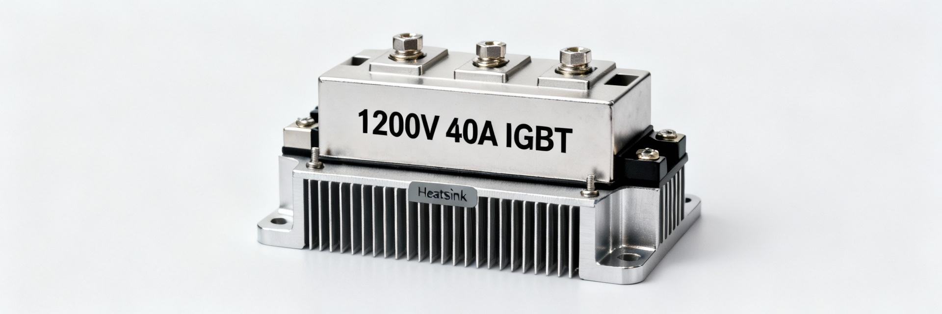
| Nominal Continuous Current | ≈ 40 A (Package dependent) | |
| Max Junction Temp (TJ) | ≥ 150°C Specification Limit | |
| Typical VCE(sat) | Specified at IC = 25–40 A | Low Loss |
Underlying Device Technology
Modern 1200 V IGBT generations use field-stop or trench techniques that trade on-state voltage against switching charge and short-circuit robustness. Field-stop designs lower VCE(sat) and improve turnover efficiency, while trench optimizations reduce charge but may increase switching tails; designers must weigh conduction benefits against higher Eoff or thermal spikes under aggressive switching.
Benchmark Methodology
Test Setup & Instruments
Recommended rig includes:
- Programmable DC bus (multiple Vbus points)
- Controllable resistive/inductive load
- Isolated gate drive with adjustable VGE
- Calibrated Rogowski or current shunt
Key Metrics & Formulas
Psw ≈ (Eon + Eoff) × fsw
ΔTJ ≈ Pdis × Rth(j-a)
Electrical Benchmarks: Conduction & Switching Losses
Conduction Performance Trends
VCE(sat) typically rises with IC and temperature. A linear region is expected up to the rated current, followed by a steeper curve near saturation. Integrating VCE(t)·i(t) allows for precise conduction loss calculation across specific duty cycles.
Switching Energy (Eon, Eoff, Erec)
Switching waveforms often highlight the Miller plateau and tail effects. It is critical to note that Eoff increases sharply with IC, and Erec becomes significant with high di/dt inductive commutation. Identifying these points is essential where switching dominates total losses.
Thermal Performance and Limits
Junction Management
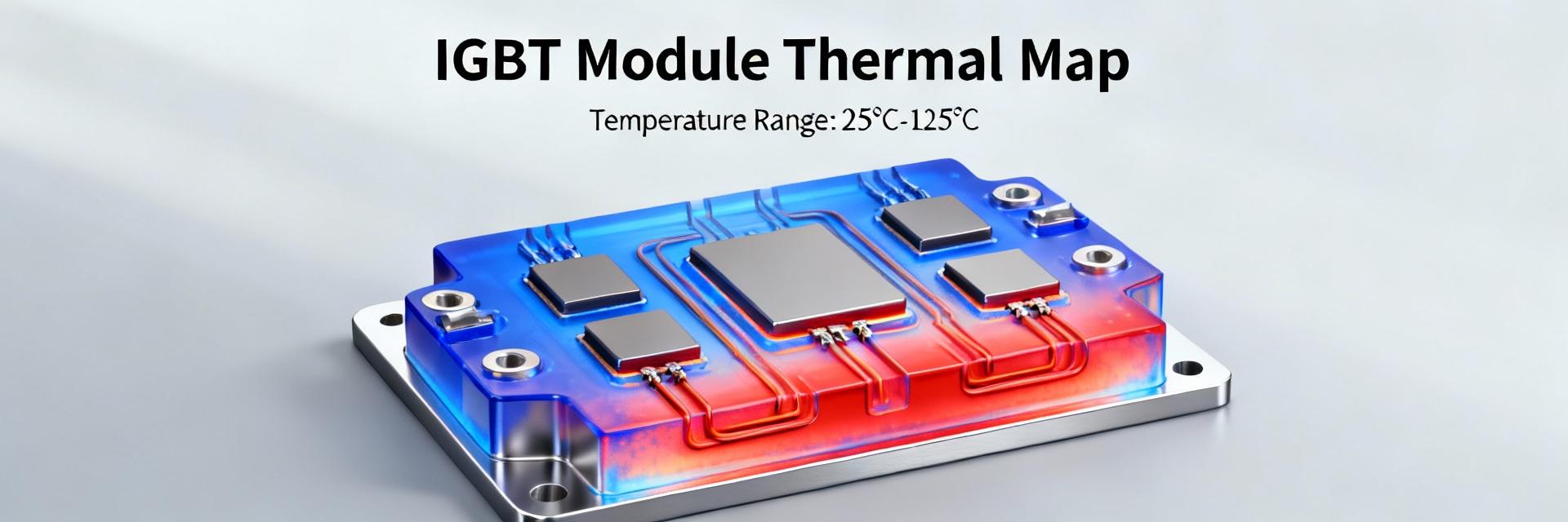
For example: 20 W dissipation with Rth(j-a) = 1.5 °C/W yields a ≈30 °C junction rise. Always use transient thermal impedance curves for pulsed losses.
Short-Circuit Capability
Withstand time must be characterized at rated VCE. Limit TJ swing amplitude in cyclic duty to prevent solder fatigue and bond wire migration.
Practical Loss-Reduction and Thermal Design Strategies
- Gate Drive Optimization: Tune gate resistors (Rg) to balance dv/dt and switching energy. Consider active Miller clamping for hard switching.
- Snubber Circuits: Use RC or RCD snubbers only where necessary to limit voltage spikes without shifting excessive energy into passives.
- Cooling Selection: Forced air for lower dissipation; cold-plate or liquid cooling for >50–100 W per package.
- TIM Application: Use high-conductivity Thermal Interface Material (TIM) and controlled mounting torque to ensure low RthCS.
Summary
Measured benchmarks show the FGH4L40T120RWD IGBT delivers competitive conduction with switching losses that must be controlled by gate drive and snubbing; thermal design is often the defining limit. Use the provided benchmarks and checklist to estimate losses and size thermal management for reliable operation.
Key Takeaways:
- Balance: Lower VCE(sat) reduces Pcond but may raise Eoff.
- Budgeting: Convert Pdis into ΔTJ via Rth(j-a) for steady-state limits.
- Repeatability: Standardize test conditions for meaningful device comparison.
Frequently Asked Questions
How do switching losses scale with current and voltage for a 1200 V / 40 A IGBT?
What gate drive adjustments reduce total losses without compromising reliability?
What are quick checks to size cooling for continuous operation?
- Technical Features of PMIC DC-DC Switching Regulator TPS54202DDCR
- STM32F030K6T6: A High-Performance Core Component for Embedded Systems
- APT50GH120B Datasheet Deep Dive: Specs, Ratings & Curves
- SI3402-B-GMR PoE PD Controller: Market & Specs Report
- SI3402-B-GMR Benchmarks: Real PoE Performance Insights
- EFM8BB21F16G Full Datasheet & Pinout: Specs Summary
- CP2102N-A02-GQFN20R Pinout & Footprint: Quick Data Guide
- SI53307-B-GMR Datasheet & CAD Models: Quick Specs Checklist
- SI53361-B-GMR: Latest Specs, Stock Levels & Price Guide
- SI53340-B-GM: Deep Performance Report & Key Metrics
-
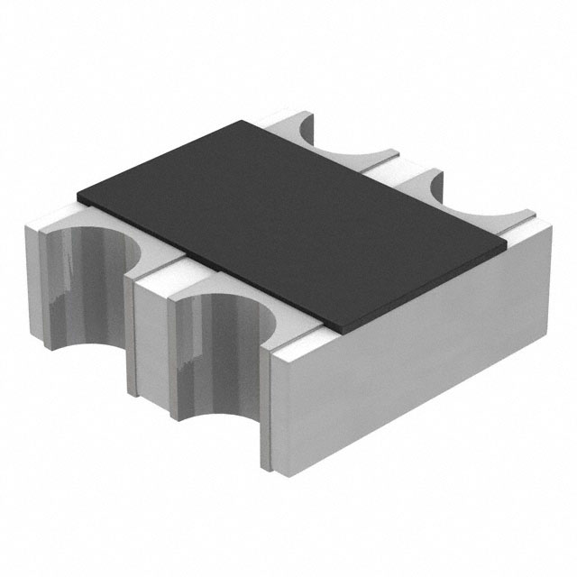 EXB-V4V120JVPanasonic Electronic ComponentsRES ARRAY 2 RES 12 OHM 0606
 -
 EXB-V4V473JVPanasonic Electronic ComponentsRES ARRAY 2 RES 47K OHM 0606
 -
 EXB-V4V823JVPanasonic Electronic ComponentsRES ARRAY 2 RES 82K OHM 0606
 -
 EXB-V4V151JVPanasonic Electronic ComponentsRES ARRAY 2 RES 150 OHM 0606
 -
 EXB-V4V181JVPanasonic Electronic ComponentsRES ARRAY 2 RES 180 OHM 0606
 -
 EXB-V4V331JVPanasonic Electronic ComponentsRES ARRAY 2 RES 330 OHM 0606
 -
 EXB-V4V152JVPanasonic Electronic ComponentsRES ARRAY 2 RES 1.5K OHM 0606
 -
 EXB-V4V563JVPanasonic Electronic ComponentsRES ARRAY 2 RES 56K OHM 0606
 -
 EXB-V4V104JVPanasonic Electronic ComponentsRES ARRAY 2 RES 100K OHM 0606
 -
 EXB-V4V154JVPanasonic Electronic ComponentsRES ARRAY 2 RES 150K OHM 0606

