-
- Contact Us
- Privacy Policy
- term and condition
- Cookies policy
EFM8BB21F16G Full Datasheet & Pinout: Specs Summary
The EFM8BB21F16G packs a 50 MHz 8‑bit core with 16 KB Flash and 2.25 KB RAM into a 3×3 mm QFN20—making it a compact, low‑power option for sensing and simple control tasks. This article provides a quick but complete datasheet summary, a pinout overview and practical design notes aimed at hardware engineers, firmware developers and procurement teams evaluating low‑cost 8‑bit microcontrollers. Estimated reading time: ~7–10 minutes. Word‑count plan: Intro ~150 words, six main sections ~150–180 words each, Summary ~140 words. Primary search phrase used in this article: "EFM8BB21F16G datasheet".
1 — EFM8BB21F16G: Overview & Where It Fits
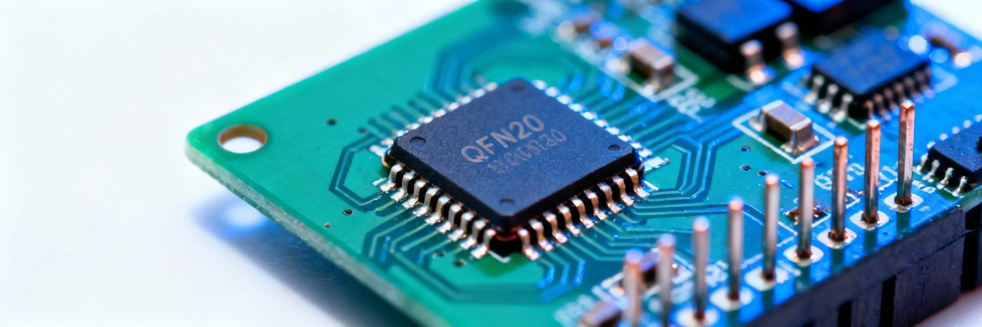
Product family context (Busy Bee series)
The EFM8BB21F16G belongs to Silicon Labs' Busy Bee (EFM8BB) family, positioned for cost‑sensitive applications that still require a solid peripheral set and low power. Busy Bee devices prioritize compact packages and efficient mixed‑signal peripherals over raw processing headroom; they are ideal where deterministic 8‑bit control is sufficient and cost, board space and power are constrained. The family shares architecture and many peripherals with downstream EFM8BB2 documentation and reference manuals, so designers benefit from consistent register models and reusable firmware patterns when migrating within the series.
Key specs snapshot (table)
The following table distills the headline specifications you will reference early in selection and BOM decisions. The caption uses the primary search phrase for on‑page relevance: "EFM8BB21F16G datasheet — quick specs".
| Parameter | Value |
|---|---|
| Core | C8051‑based 8‑bit pipelined |
| Max frequency | 50 MHz |
| Flash | 16 KB |
| RAM | 2.25 KB |
| GPIO / usable I/O | Up to 16 |
| ADC | 12‑bit |
| Timers | Multiple 16‑bit timers, PCA |
| Supply | 2.2 – 3.6 V |
| Temperature | −40 to 85 °C |
| Package | QFN20, 3×3 mm |
Typical use cases
Typical deployments include sensor nodes, keypad controllers, simple motor or actuator control, and low‑cost consumer devices. The combination of a 50 MHz core, 12‑bit ADC and multiple 16‑bit timers makes the part well suited to mixed‑signal edge tasks where precise timing and modest analytics are required, but where a 32‑bit MCU would be overkill in cost, power or board area.
2 — Full Specs Breakdown (Core, Memory, Power)
CPU, clocks, and performance
The device uses a C8051‑derived 8‑bit pipelined core with single‑cycle and multi‑cycle instructions depending on the operation; peak external bus/flash fetches and internal peripherals run with a 50 MHz system clock. Designers can select internal oscillators or an external crystal; recommended clock sources include the factory‑trimmed internal HF oscillator for low BOM and a low‑frequency crystal for low jitter timing. For common tasks—UART at 115.2 kbps, ADC sampling and simple control loops—developers should budget CPU cycles for ADC conversions and ISR overhead; real‑time loops at tens of kilohertz are practical, but complex DSP‑style math or heavy string processing will push the 8‑bit architecture toward its limits.
Memory: Flash, RAM, and storage
Flash is 16 KB total; typical memory maps partition a small boot/loader region and the remainder for application code. RAM is 2.25 KB—adequate for modest stacks, buffers and small RTOS‑free firmware. The device lacks large embedded file system support; EEPROM emulation patterns using Flash pages are common if nonvolatile data beyond simple parameter storage is required. For OTA or field upgrades, reserve staging sectors and include CRC or dual‑bank checks to protect update integrity; plan code size and stack use aggressively given the 16 KB limit.
Power, supply ranges, and low‑power modes
Supply range is 2.2–3.6 V, enabling single‑cell Li‑ion or 3.3 V systems. Low‑power modes include reduced clock and standby states that stop most peripherals while retaining RAM or selective wake sources such as GPIO, comparator or RTC timers. For battery designs, pay attention to standby leakage and wake latencies; add a local LDO or buck converter tuned to the MCU's active/standby profile. Standard decoupling (0.1 μF close to VDD pins plus a 4.7 μF bulk) and ferrite or LC filtering are recommended for noisy power rails to preserve ADC accuracy and RF immunity for nearby radios.
3 — Peripherals: ADC, Timers, Communication & GPIO
Analog & ADC
The on‑chip ADC is 12‑bit with multiple channels and selectable sample times and references. Input ranges follow the supply and internal reference options—designers can use the internal bandgap or an external reference for improved accuracy. For low‑noise analog readings, place the ADC input traces away from PWM and clock lines, use ground pours with a single quiet analog ground return, and place bypass capacitors at the ADC reference pin. Typical sampling strategies include averaging and oversampling to improve effective resolution in noisy environments.
Timers, PCA and PWM
Timing resources include several 16‑bit general timers and a programmable counter array (PCA) with multiple capture/compare channels for PWM generation. Typical uses are precise motor control, LED dimming and ultrasonic timing. With a 50 MHz clock and prescalers, you can get microsecond resolution for short pulses and millisecond resolution for longer intervals. Examples: 16‑bit timer at no prescale gives ~1.3 ms overflow; with a prescaler of 64 you get longer intervals but lower resolution—pick prescalers to balance resolution and ISR frequency.
Digital comms: UART, SPI, I2C and GPIO
The part supports UART, SPI and I2C‑style interfaces mapped to configurable pins; multiple serial ports enable sensor aggregation and debug channels simultaneously. Up to ~16 usable GPIO lines provide flexible multiplexing into ADC channels or serial functions; check the datasheet for any pins with 5 V tolerance—some I/O may be 5 V tolerant while others are not. Use isolated debug UARTs for field diagnostics and reserve at least one UART or SPI interface for firmware upgrade paths when possible.
4 — Pinout & Package Details (Pin Map + PCB Tips)
QFN20 pin mapping (pin‑by‑pin)
Below is a practical pin map summary that reproduces the official 20‑pin QFN layout in a compact table form—each entry shows pin number, name, primary type and common alternate functions so designers can place critical signals and plan ground/thermal connections. For distribution and CAD use, keep an SVG/PNG of the official artwork in your design library and name the asset "EFM8BB21F16G pinout diagram" for clarity.
| Pin | Name | Type / Alt functions |
|---|---|---|
| 1 | P0.0 | GPIO / ADC |
| 2 | P0.1 | GPIO / UART / SPI |
| 3 | P0.2 | GPIO / PCA |
| 4 | VDD | Power |
| 5 | GND | Ground |
| 6 | RESET | Reset / debug |
| 7 | XTAL_P | Crystal |
| 8 | XTAL_N | Crystal |
| 9 | P1.0 | GPIO / I2C |
| 10 | P1.1 | GPIO / ADC |
| 11 | P1.2 | GPIO / PWM |
| 12 | VSS (EP) | Exposed pad / GND |
| 13 | P2.0 | GPIO / SPI |
| 14 | P2.1 | GPIO / UART |
| 15 | P2.2 | GPIO / ADC |
| 16 | P2.3 | GPIO |
| 17 | P3.0 | GPIO / PCA |
| 18 | P3.1 | GPIO / PWM |
| 19 | VDD | Power |
| 20 | GND | Ground |
Package, footprint and mechanical data
The QFN20 package is 3×3 mm with an exposed thermal ground pad; designers should follow the manufacturer's recommended land pattern and stencil apertures to ensure reliable solder joints and thermal performance. Use thermal pad stitching to connect the exposed pad to multiple ground vias; keep the pad size consistent with the mechanical drawing and place at least four 0.3–0.4 mm diameter via stitches in the pad that are tented or filled per your boardhouse capability to avoid solder wicking issues.
PCB layout & soldering recommendations
For robust soldering: place 0.1 μF decouplers within 1–2 mm of VDD pins, tie analog grounds separately and join at a single point near the exposed pad, and use 6–12 ground vias around the thermal pad for heat dissipation and return paths. Keep ADC inputs short, use guard traces if necessary, and route noisy PWM traces away from analog routes. Reflow profiles should follow standard lead‑free profiles with controlled ramp rates to protect the package and nearby passives.
5 — Development Tools, Programming & Debugging
IDEs, toolchains and sample code
Supported toolchains include Silicon Labs' Simplicity Studio, and common third‑party options such as Keil and SDCC. The vendor provides example projects for clock configuration, UART echo tests and ADC sampling that are suitable as first smoke tests on a new board. For firmware onboarding, start with minimal examples that: 1) initialize clock and GPIO, 2) toggle an LED on a timer interrupt, and 3) perform periodic ADC reads and report over UART—these validate power, clock and peripheral wiring quickly.
Debugging interfaces & bootloader
Debug access typically uses Silicon Labs' C2 debug interface or vendor‑specific connectors; verify the exact debug pin mapping on your package variant. The device supports a bootloader mode—enterable via reset pin sequence or software request—useful for field programming. Common debug scenarios involve verifying clock source frequency, checking vector table locations, and halting in ISRs to check stack usage; keep a UART console or LED patterns to signal early boot status when a debugger is not available.
Reference documents & where to download the datasheet
Designers should obtain the official product page, full datasheet PDF and the Busy Bee family reference manual from the manufacturer for exact register maps, mechanical drawings and electrical characteristics—copy exact filenames for documentation traceability in your design files. Important figures to capture in your design pack include the pinout graphic, maximum ratings table and recommended footprint drawing; place these in your PCB library and BOM notes for review and manufacture.
6 — Selection Checklist & Design Considerations
Comparing alternatives & selection criteria
Choose the EFM8BB21F16G when your design needs a compact, low‑cost 8‑bit MCU with modest memory and a strong mixed‑signal peripheral set. If you require more Flash/RAM, additional I/O or higher throughput for complex algorithms, consider larger EFM8 parts or a low‑end ARM Cortex‑M device. Key criteria: required code size, RAM buffers, ADC accuracy, number of serial interfaces and package constraints. Use a simple decision matrix weighing cost, performance and PCB area to guide the final selection.
BOM, sourcing and lead‑time tips
Preferred ordering codes follow manufacturer nomenclature for QFN and alternate packages; include tape‑and‑reel part numbers in your BOM for volume builds and track distributor lead times early. Use authorized distributors and watch for suspiciously low‑priced, loose devices to avoid counterfeits; require certificate of conformity from suppliers when massing orders. Reserve alternate package options (QSOP, etc.) in your BOM to mitigate supply risk.
Thermal, EMC and reliability checklist
Run a quick checklist before sign‑off: thermal derating analysis for continuous active current, add local decoupling and common‑mode filtering for EMC, isolate ADC inputs from switching nodes, and include ESD protection on exposed I/O. For harsh environments, consider conformal coating and choose passives rated for expected ambient ranges; document test cases and margin requirements for long‑term reliability.
Summary
For compact 8‑bit control with modest memory and a solid peripheral set, the EFM8BB21F16G is a practical choice that balances cost, size and mixed‑signal capability—consult the official EFM8BB21F16G datasheet and pinout diagram before PCB design to confirm exact electrical and mechanical constraints. The main takeaway: validate memory needs against the 16 KB Flash / 2.25 KB RAM limit, reserve interfaces for firmware upgrades and debugging, and follow thermal/footprint recommendations for reliable QFN20 assembly. Primary search phrase referenced here: "EFM8BB21F16G datasheet".
Quick selection highlights
- Compact QFN20 with 16 KB Flash—best for minimal‑footprint sensor/control nodes.
- 50 MHz 8‑bit core with 12‑bit ADC—good for precise sensing and timing tasks.
- Supply 2.2–3.6 V—battery‑friendly; plan decoupling and low‑power modes carefully.
- Reserve UART/SPI for bootloader and diagnostics; map critical ADC pins away from noisy traces.
Frequently Asked Questions
Is the EFM8BB21F16G suitable for low‑power battery operation?
Yes. With a 2.2–3.6 V supply range and several low‑power modes, the device can be configured for battery operation. Designers should profile active and standby currents using representative code, enable low‑power oscillator options, and ensure wake sources are limited to required signals to maximize battery life. Add 0.1 μF plus 4.7 μF decoupling near VDD and consider a low‑Iq regulator for single‑cell applications.
Where can I find the official EFM8BB21F16G pinout and mechanical drawings?
The official pinout graphic and mechanical drawing are provided in the manufacturer's product documentation and datasheet PDF; include these assets in your PCB library and follow the recommended land pattern and exposed pad guidelines. Use the manufacturer drawing to set solder paste apertures and via‑in‑pad policies to avoid assembly issues.
Can I use this part for simple motor control and PWM dimming?
Yes. The PCA channels and multiple 16‑bit timers support PWM use cases for small motors and LED dimming. Be mindful of switching noise coupling into ADC channels; place PWM outputs and drivers on separate copper pours where possible and use snubbers or MOSFET gate resistors to limit EMI for cleaner analog readings.
- Technical Features of PMIC DC-DC Switching Regulator TPS54202DDCR
- STM32F030K6T6: A High-Performance Core Component for Embedded Systems
- APT50GH120B Datasheet Deep Dive: Specs, Ratings & Curves
- SI3402-B-GMR PoE PD Controller: Market & Specs Report
- SI3402-B-GMR Benchmarks: Real PoE Performance Insights
- EFM8BB21F16G Full Datasheet & Pinout: Specs Summary
- CP2102N-A02-GQFN20R Pinout & Footprint: Quick Data Guide
- SI53307-B-GMR Datasheet & CAD Models: Quick Specs Checklist
- SI53361-B-GMR: Latest Specs, Stock Levels & Price Guide
- SI53340-B-GM: Deep Performance Report & Key Metrics
-
 EXB-V4V120JVPanasonic Electronic ComponentsRES ARRAY 2 RES 12 OHM 0606
 -
 EXB-V4V473JVPanasonic Electronic ComponentsRES ARRAY 2 RES 47K OHM 0606
 -
 EXB-V4V823JVPanasonic Electronic ComponentsRES ARRAY 2 RES 82K OHM 0606
 -
 EXB-V4V151JVPanasonic Electronic ComponentsRES ARRAY 2 RES 150 OHM 0606
 -
 EXB-V4V181JVPanasonic Electronic ComponentsRES ARRAY 2 RES 180 OHM 0606
 -
 EXB-V4V331JVPanasonic Electronic ComponentsRES ARRAY 2 RES 330 OHM 0606
 -
 EXB-V4V152JVPanasonic Electronic ComponentsRES ARRAY 2 RES 1.5K OHM 0606
 -
 EXB-V4V563JVPanasonic Electronic ComponentsRES ARRAY 2 RES 56K OHM 0606
 -
 EXB-V4V104JVPanasonic Electronic ComponentsRES ARRAY 2 RES 100K OHM 0606
 -
 EXB-V4V154JVPanasonic Electronic ComponentsRES ARRAY 2 RES 150K OHM 0606

