-
- Contact Us
- Privacy Policy
- term and condition
- Cookies policy
SNXH150B95H3Q2F2PG-N datasheet: electrical & thermal specs
Functional Role & Package
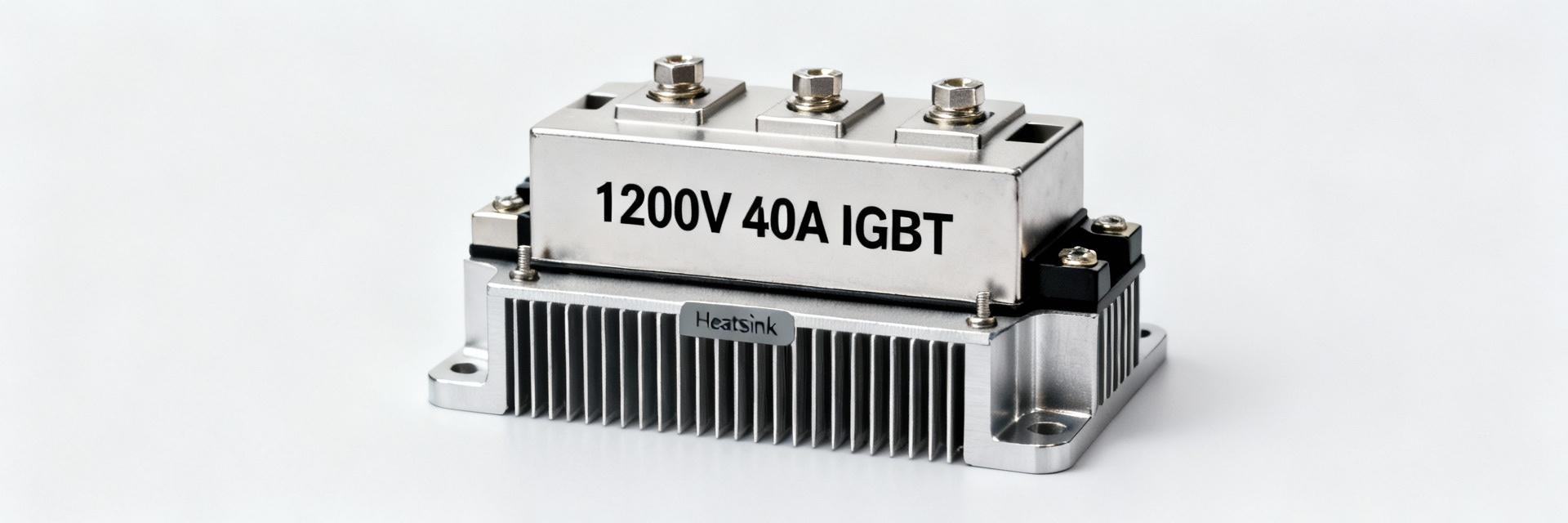
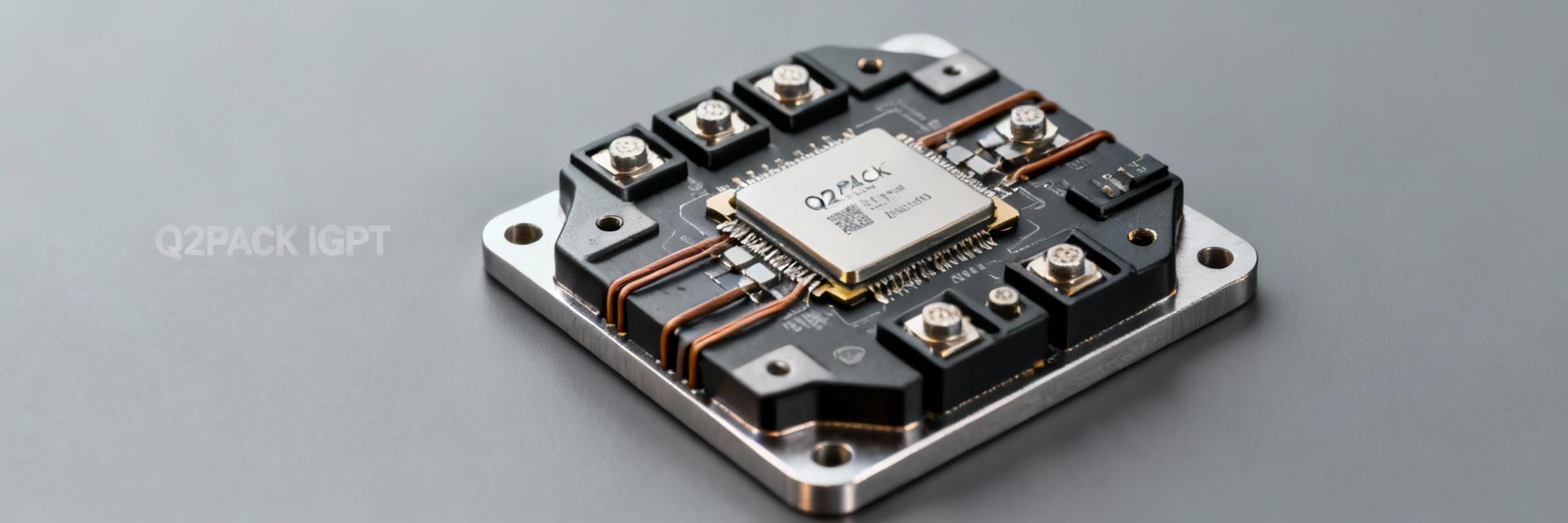
Point: The device is a high-current power switch intended for power‑conversion or load‑switch applications, offered in a multi-pin power package with dedicated collector/emitter and thermal pad.
Evidence: The datasheet groups functional description, pinout, and package drawings at the front, followed by electrical ratings and switching characteristics.
Explanation: Consult the initial pages for package/pin assignments, the absolute‑maximum ratings table for DC limits, and the electrical characteristics and switching tables for dynamic behavior.
Conditions & Footnotes to Watch
Point: Datasheet numbers depend on test conditions—common defaults are TJ = 25°C for characteristic curves.
Evidence: Footnotes typically specify pulse duration, duty cycle, or waveform used for capacitance measurements.
Explanation: Verify whether a rating is an absolute maximum or a recommended operating condition. Use derating curves to convert single‑point values to your specific operating environment.
Electrical Specifications: Data Deep-Dive
DC Limits & Absolute Maximum Ratings
Extract VCE (or VDS for MOSFETs), continuous collector current, pulsed current, and maximum junction temperature. Design Note: Use absolute maximums only for stress‑test planning. Maintain significant headroom between worst‑case operating voltage and absolute limits to ensure longevity.
Dynamic Characteristics & Parasitics
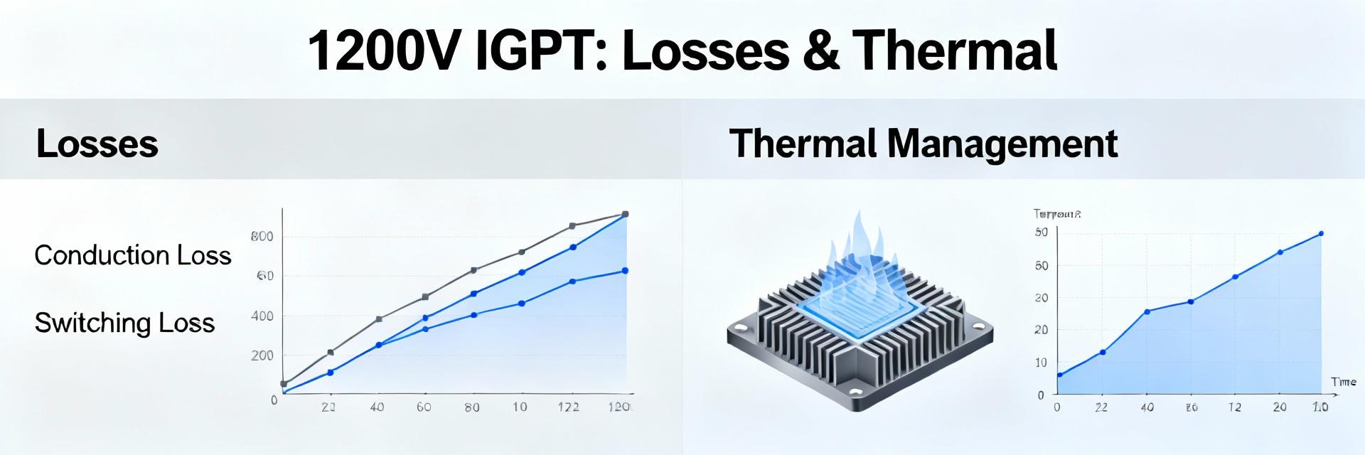
Important items include input/output capacitances (Ciss/Coss/Crss) and switching times. Design Note: High input capacitance increases gate‑drive charge. Size the gate driver to deliver required dQg/dt and include series resistance to control EMI.
Thermal Specifications & Management
Practical Thermal Guidance
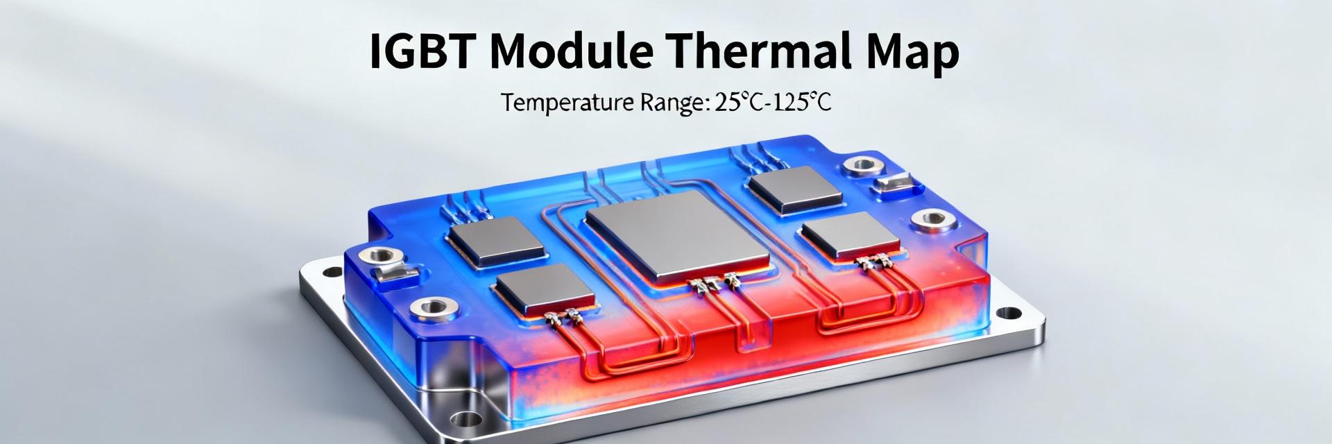
Achieving thermal targets requires integrated mechanical decisions. Minimize Thermal Interface Material (TIM) thickness and maximize copper pours under the package. For transient pulses, verify junction temperature rise using single‑pulse energy limits rather than steady‑state power dissipation (Pd).
Design Case Study: 200W Switching Stage
Application Workflow: 50V Nominal System
*Example Calculation: Determine worst‑case Vdrop and switching energy. Use ΔT = Pd × RθJA to confirm Tj_max margin. If insufficient, plan for forced airflow.
Measurement, Verification & Test Best Practices
Lab Validation
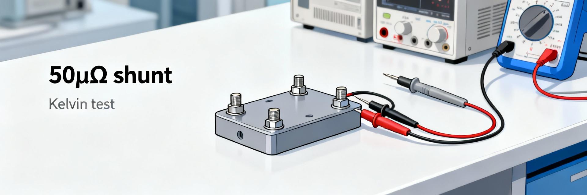
- Use low‑inductance Kelvin connections for Vce(sat).
- De‑embed probe capacitance for accurate dynamic tests.
- Minimize loop areas to mitigate parasitic noise.
Reliability Checks
- Perform IR thermography on calibrated surfaces.
- Execute repeated pulse and thermal‑cycle tests.
- Include TIM reproducibility checks in pass/fail criteria.
Key Summary
- ✓ Extract absolute‑maximum V and I; design with derating margins to avoid thermal runaway.
- ✓ Use datasheet capacitances to size gate drivers and estimate switching losses.
- ✓ Perform a thermal budget using Tj = Ta + Pd × RθJA.
- ✓ Validate in the lab using low‑parasitic setups and empirical thermal measurements.
Common Questions and Answers
- Technical Features of PMIC DC-DC Switching Regulator TPS54202DDCR
- STM32F030K6T6: A High-Performance Core Component for Embedded Systems
- APT50GH120B Datasheet Deep Dive: Specs, Ratings & Curves
- SI3402-B-GMR PoE PD Controller: Market & Specs Report
- SI3402-B-GMR Benchmarks: Real PoE Performance Insights
- EFM8BB21F16G Full Datasheet & Pinout: Specs Summary
- CP2102N-A02-GQFN20R Pinout & Footprint: Quick Data Guide
- SI53307-B-GMR Datasheet & CAD Models: Quick Specs Checklist
- SI53361-B-GMR: Latest Specs, Stock Levels & Price Guide
- SI53340-B-GM: Deep Performance Report & Key Metrics
-
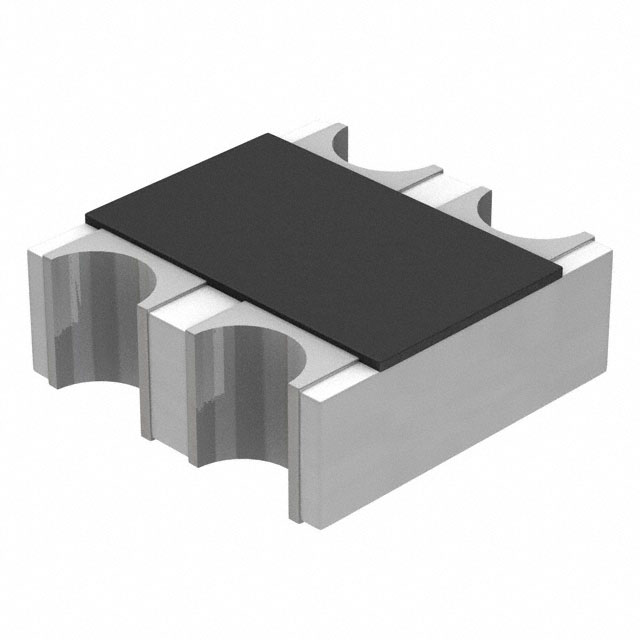 EXB-V4V120JVPanasonic Electronic ComponentsRES ARRAY 2 RES 12 OHM 0606
 -
 EXB-V4V473JVPanasonic Electronic ComponentsRES ARRAY 2 RES 47K OHM 0606
 -
 EXB-V4V823JVPanasonic Electronic ComponentsRES ARRAY 2 RES 82K OHM 0606
 -
 EXB-V4V151JVPanasonic Electronic ComponentsRES ARRAY 2 RES 150 OHM 0606
 -
 EXB-V4V181JVPanasonic Electronic ComponentsRES ARRAY 2 RES 180 OHM 0606
 -
 EXB-V4V331JVPanasonic Electronic ComponentsRES ARRAY 2 RES 330 OHM 0606
 -
 EXB-V4V152JVPanasonic Electronic ComponentsRES ARRAY 2 RES 1.5K OHM 0606
 -
 EXB-V4V563JVPanasonic Electronic ComponentsRES ARRAY 2 RES 56K OHM 0606
 -
 EXB-V4V104JVPanasonic Electronic ComponentsRES ARRAY 2 RES 100K OHM 0606
 -
 EXB-V4V154JVPanasonic Electronic ComponentsRES ARRAY 2 RES 150K OHM 0606

