-
- Contact Us
- Privacy Policy
- term and condition
- Cookies policy

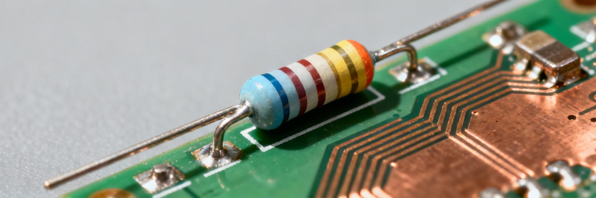
4310R-101-222: Complete Spec Breakdown & Performance Data
22 January 2026
0
Related articles
-
 WSBR8536L0500JKA4: Specs & Thermal Data for 50W Shunt2026-01-24 12:47:43 0At a nominal resistance of 50 µΩ and a 50 W power rating, the WSBR8536L0500JKA4 has a theoretical peak dissipation current of ~1000 A (I = sqrt(P/R)), making it a candidate for high‑current sensing in battery and power‑distribution systems — but practical continuous current depends on mounting and cooling. This article translates datasheet numbers into electrical and thermal calculations, measurement/test methods, integration guidance, and a concise sizing checklist for power electronics designers, BMS engineers, and test technicians. It also highlights lab procedures to verify continuous ratings and recommendations for reliable Kelvin sensing and calibration for a 50W shunt. This guide assumes designers will reference the official product documentation for exact TCR, tolerance and mechanical torque values; where appropriate, it recommends measurement methods and derating. Practical examples use common currents (100 A–1000 A) so teams can map sense voltage, dissipated power, and expected thermal rise before committing to fixtures or production layouts. Quick Overview & Intended Applications (background) Part identity & baseline specs Essential nominal specs to extract from the datasheet include: nominal resistance = 50 µΩ, resistance tolerance (commonly ±5% or as specified), rated power = 50 W, operating temperature range, mounting type and fixture pitch, recommended bolt size and torque, and whether the package is single‑ or dual‑element for redundancy. Quote exact datasheet values verbatim during design reviews and note any family variants with different power or tolerance specs so parts are not interchanged improperly. Typical use-cases & system roles Common applications are battery current sensing, EV high‑current bus monitoring, power‑supply inrush measurement and energy metering where low voltage drop and robustness are required. A low‑ohm 50 W shunt is chosen where millivolt‑level sense voltages are acceptable and where cost, linearity and low TCR are priorities versus hall or magnetic sensing. Consider WSBR8536L0500JKA4 for battery management evaluation where mechanical mounting and thermal path are well controlled. Electrical Specs & Practical Calculations (data analysis) // Core Formulas I_max_theoretical = sqrt(P/R) V = I × R P = I² × R For R = 50 µΩ and P = 50 W, I_max ≈ 1000 A (theoretical, assuming resistor dissipates full rated power). Voltage drops: 100 A → 5 mV; 500 A → 25 mV; 1000 A → 50 mV. Power examples: 500 A → 12.5 W; 750 A → 28.1 W. Use these to size amplifier gain and ADC range. Current (A) Vdrop (mV) Power (W) % of Rated Power 100 5.0 0.5 1% 500 25.0 12.5 25% 750 37.5 28.1 56% 1000 50.0 50.0 100% Accuracy, tolerance & measurement margin Tolerance (for example ±5%) and TCR determine absolute error across temperature. At millivolt sense levels, amplifier input offset and ADC LSB size dominate measurement accuracy. For a 5–50 mV range, recommend instrumentation amplifiers with microvolt offset specs and drift below the shunt TCR×ΔT. Typical guidance: aim amplifier gain so full‑scale ADC input is 50–80% of ADC range, and use 16‑bit or better ADCs for sub‑0.1% resolution on lower currents. Derate continuous dissipation and allow margin for tolerance and drift. Thermal Behavior & Test Methods (data analysis + method) Thermal calculations & expected temperature rise Key thermal metric: element‑to‑ambient thermal resistance θ (°C/W). Convert dissipation to temperature rise with ΔT = P × θ. Use P = I²R to plot ΔT vs current and present a sample curve. Note that datasheet power ratings commonly assume a specified fixture and airflow; an identical part in a different fixture can see substantially higher ΔT. Always verify θ either from datasheet or by measurement on the intended mounting hardware. Recommended Lab Checklist ✔ Apply controlled current ramps while recording element temperature with thermocouples. ✔ Run steady‑state power soak tests at 25%, 50% and 75% of theoretical I_max. ✔ Log Vsense, ambient, element temp and time‑to‑stable. ✔ Verify bolting torque and thermal contact integrity. Integration & Sensing Best Practices (method) Mechanical & PCB Design Minimize thermal resistance by ensuring flat, clean contact between shunt and fixture, using recommended bolt torque from the datasheet. Provide conduction paths (thick busbars or heat spreaders) and consider forced‑air cooling for continuous high dissipation. Arrange spacing and clearance for safe creepage and short Kelvin sense leads routed to the amplifier; avoid thin PCB traces in the main current path to reduce parasitic resistance and heating. Electrical & Calibration Use true Kelvin (4‑wire) connections: two heavy current terminals and two separate sense leads to the amplifier. Select amplifiers with common‑mode range that accommodates bus voltages and add input filtering to reject transients. Calibration routine: remove zero‑offset, characterize temperature drift across representative ambient range, and schedule periodic recalibration. For continuous operation, design for 60–80% of rated dissipation. Application Examples, Sizing Checklist & Troubleshooting (case + action) Example Scenarios Example 1 — 200 A continuous: Vdrop = 200 × 50 µΩ = 10 mV P = 200² × 50 µΩ = 2.0 W (4% of 50 W). Example 2 — 600 A peak (10% duty): Peak P = 18.0 W (36%) Average P over duty cycle ≈ 1.8 W (3.6%). Troubleshooting common issues High drift — verify TCR and improve thermal coupling to fixture. Noise on sense line — shorten Kelvin leads, add common‑mode filtering and differential input filtering. Excessive temperature rise — increase conduction area, add forced air, or reduce continuous duty. Field checklist: measure Vsense, shunt body temperature, bolt torque, and compare to baseline graphs to flag deviations. Summary & Next Steps The WSBR8536L0500JKA4 nominal 50 µΩ / 50 W rating implies theoretical high‑current capability (~1000 A), but practical continuous use depends on thermal path, mounting and derating. Proceed with the following checklist before production: Verify quoted specs from the datasheet (resistance, tolerance, TCR and torque) before layout. Use P = I²R and ΔT = P×θ to plot thermal rise and choose fixture cooling. Implement Kelvin wiring and select low‑offset amplifiers for the 5–50 mV range. Run controlled soak tests at 25/50/75% of theoretical peak current. Frequently asked questions How do I calculate the expected voltage drop for a given current? + Use V = I × R. For a 50 µΩ nominal resistance, multiply the current in amps by 50×10⁻⁶ to get volts (e.g., 500 A → 25 mV). Use the part tolerance and TCR to estimate variation across temperature and include amplifier offset in accuracy budgets. What test steps verify continuous power capability? + Perform controlled current ramps and steady‑state soak tests while measuring element temperature with thermocouples and thermal imaging. Run tests at representative currents (e.g., 25%, 50%, 75% of theoretical peak), log time‑to‑stable, Vsense and ambient, and compare ΔT to the expected P×θ curve. Verify consistent results after multiple cycles. How should I size the amplifier and ADC for millivolt sense signals? + Choose amplifier gain so peak sense voltage uses 50–80% of ADC full scale; pick amplifiers with microvolt offset and low drift. For typical 5–50 mV ranges, a 16‑bit ADC with proper input range and anti‑alias filtering provides adequate resolution; always budget for tolerance, TCR drift and noise when selecting gain and filter time constants. /* Adding basic keyframes for the H5 animations requested */ @keyframes slideDown { from { opacity: 0; transform: translateY(-10px); } to { opacity: 1; transform: translateY(0); } } /* Ensuring list markers look clean as requested */ li::marker { color: #0056b3; font-weight: bold; } /* Better responsiveness for table */ @media (max-width: 768px) { table th, table td { padding: 8px !important; font-size: 13px; } h1 { font-size: 24px !important; } }READ MORE
 -
 8BRN10K Resistor Network: Live Stock, Pricing & Specs2026-01-23 12:32:39 0@keyframes fadeInUp { from { opacity: 0; transform: translateY(20px); } to { opacity: 1; transform: translateY(0); } } @keyframes fadeInDown { from { opacity: 0; transform: translateY(-20px); } to { opacity: 1; transform: translateY(0); } } @keyframes pulse { 0% { transform: scale(1); } 50% { transform: scale(1.02); } 100% { transform: scale(1); } } summary::-webkit-details-marker { display: none; } li::marker { color: #3498db; font-size: 1.2em; } Introduction 8BRN10K Resistor Network: Live Stock, Pricing & Specs. Market signals show spot availability varying between distributors and marketplace sellers, with single-unit prices clustered in a narrow band while bulk pricing drops noticeably at MOQs of 100 or more. Timely stock and pricing intel prevents BOM delays and costly last-minute substitutions for buyers and design engineers. This guide delivers practical live-stock checking tactics, pricing benchmarks and actionable spec guidance for the Resistor Network so teams can set alerts, compare channels and validate critical datasheet parameters before placing orders. Background: What the 8BRN10K Resistor Network Is Point: The 8BRN10K is an eight-element resistor array typically offered as a compact SIP package for signal bussing and pull-up grids. Evidence: It’s sold as bussed and isolated variants with 10 kΩ nominal elements. Explanation: Designers choose it to reduce board area and assembly time versus discrete resistors while keeping consistent element values across a common package. Key electrical characteristics to state up front Nominal resistance: 10 kΩ; defines divider or pull-up value and input bias behavior. Number of resistors: 8 elements; determines channel count for multi-line bussing. Circuit type: Bussed vs. isolated; bussed shares a common pin, isolated has independent pins. Power per element: Typical 1/8W to 1/4W; sets continuous current limits. Tolerance: Common 1%–5%; affects matching and pull-up precision. Temperature coefficient: Tens to hundreds ppm/°C; dictates drift over operating range. Each parameter directly influences selection risk: tolerance and TCR affect signal accuracy, power rating affects thermal derating, and circuit type affects PCB routing and verification steps. Typical packages and footprint details Common formats include SIP-8 and SIP-9 variations with 2.54 mm pitch and 7–12 mm body lengths. Designers should confirm pin numbering and common-pin location before layout. Package Pitch Typical Body Length SIP-8 (bussed) 2.54 mm 8–10 mm SIP-9 (isolated) 2.54 mm 9–12 mm Live stock & pricing snapshot for 8BRN10K Point: Live stock fluctuates between authorized distribution and secondary marketplaces; timestamped checks matter. Evidence: At any moment listings show a range of quantities and lead times across channels. Explanation: Capture timestamp, seller channel, qty available, unit price and lead time to create a short-term price/availability snapshot for procurement decisions. How to check live stock reliably (methodology) Query distributor inventory feeds and marketplace listings, search by exact part number and common alternate phrases, and record lead-time fields labeled in-stock, backorder or ETA. Capture timestamp, available qty, unit price and MOQ and archive page screenshots or CSV exports to support price-trend tracking and supplier follow-up. Pricing patterns & what to expect Single-unit prices often sit within a tight band; expect discounts when ordering 100+ units. Marketplace sellers typically carry a markup for small quantities while distribution channels offer clearer tiered pricing. Quantity Range (MOQ) Typical Unit Price (Estimate) Cost Intensity 1–9 Units Highest, Marketplace Premium 10–99 Units Moderate 100+ Units Lowest per-unit Specs deep-dive: interpreting datasheets and key tolerances Prioritize tolerance, power per element, TCR (ppm/°C), max working voltage and noise figures on datasheets. These parameters indicate drift, thermal limits and suitability for analog vs. digital contexts. Datasheet Priorities Example BOM note phrasing: “Confirm 10 kΩ, 1/8W per element, 5% tolerance, 100 ppm/°C TCR, bussed configuration” — this focuses procurement and QA on the specs that matter for design risk. Test & Verification Verify arrays both in-circuit and out-of-circuit; confirm common-pin continuity on bussed parts, measure element resistance spread, and apply derating guidelines for elevated temperatures. Buying & sourcing playbook Sourcing Tactics Checklist: Match 10 kΩ, 8 elements, circuit type, power, and pinout. Do: Confirm pin mapping and TCR. Don’t: Swap bussed for isolated without layout change. Search phrase: “10k 8-element bussed SIP resistor network”. Ordering Strategy Buy samples for first-run builds, split production orders into immediate and scheduled replenishment batches. Negotiate packaging or MOQ where possible. Maintain a short approved-equivalents list. Sample inquiry: "Request current available qty, lead time, unit price and MOQ for part number; please confirm datasheet revision." Applications, design notes & replacement scenarios Use resistor arrays for pull-up banks, signal bussing and level-shift networks to save board space. Arrays reduce assembly steps and improve matching across channels. Common use cases Typical uses include pull-up grids on microcontroller ports, resistor ladders for level shifting and matched input terminations. Wiring example: each resistor connects from pin to common pull-up pin for open-drain inputs. How to choose an alternative (OOS Scenario) First match resistance and topology, then per-element power and package pinout. Verify mechanical fit and TCR; prototype-test any substitute. Search long-tail: “8BRN10K alternative resistor network” or “8-element 10k bussed SIP”. Summary ✔ Live-stock checks should capture timestamped qty, unit price, MOQ and lead time so buyers can compare channels and track price trends before committing to orders for the 8BRN10K Resistor Network. ✔ Prioritize tolerance, per-element power and TCR from datasheets; these specs govern drift, derating and suitability for analog vs. digital tasks. ✔ Procurement tactics: buy samples, split orders, set alerts and prefer distribution tier pricing for bulk buys while using marketplace listings for urgent small-quantity needs. Frequently Asked Questions How can I quickly verify 8BRN10K stock availability? ▼ Check distributor inventory feeds and marketplace listings with exact part numbers and alternate search phrases, capture timestamped screenshots or CSV exports and record available qty, unit price, MOQ and lead time. Automate alerts where possible and archive checks to observe short-term trends and spot markup patterns. What are the minimal datasheet specs to confirm before ordering? ▼ Confirm nominal resistance (10 kΩ), circuit type (bussed vs. isolated), per-element power rating, tolerance and temperature coefficient. These determine electrical fit, thermal limits and drift; noting them in BOM entries reduces risk of receiving mismatched parts for production runs. When is it acceptable to substitute a different resistor network? ▼ Substitution is acceptable only after verifying the substitute matches resistance, topology and pinout, then confirming equal or superior power rating and TCR. Prototype-test substitutes for electrical and mechanical fit before approving them for full production to avoid rework or failures.READ MORE
 -
 10K 10-Pin SIP Resistor Network: Complete Specs Guide2026-01-21 12:36:49 0Engineers specifying resistor arrays rely on precise electrical and mechanical data to prevent field failures. This comprehensive guide decodes critical specifications, selection criteria, and thermal management for embedded, analog, and industrial designs. ? What is a 10k Resistor Network in a 10-Pin SIP? A 10-pin Single In-Line Package (SIP) integrates multiple resistors into a compact, space-saving footprint. Typical per-resistor power ratings are around 1/8 W (≈125 mW), with tolerances ranging from ±1% to ±5%, and temperature coefficients between ±50 and ±250 ppm/°C. Form Factor & Pinout A 10-pin SIP packages ten individual resistors with a 2.54 mm (0.1") pitch. The overall length is typically ≲25.4 mm. We recommend a through-hole footprint with 0.8–1.0 mm plated holes and 2.8–3.2 mm pad lengths. [1 2 3 4 5 6 7 8 9 10] | | | | | | | | | | (Top View Pin Row) Internal Configurations Isolated: 10 independent elements. Bussed: 9 resistors tied to a common pin. Ladder: Used for R-2R DAC/ADC networks. Series: Connected in a single string for termination. Key Electrical Performance Metrics Power Rating (Per Element) 125 mW - 250 mW Temperature Coefficient (Tempco) ±50 – ±250 ppm/°C Pro Tip: Calculate allowable current using I = sqrt(P/R). For 125 mW into 10 kΩ, I_max ≈ 3.5 mA. Ensure derating for ambient temperatures above 70°C. Reliability & Stability Drift over time depends on the resistance film technology. Thick-film components are cost-effective for non-critical pull-ups, while thin-film variants offer superior long-term stability and lower aging (often expressed in ppm/year) for precision ADC dividers. Environmental Performance Standard operating ranges span −55°C to +125°C. Optional conformal coatings protect against moisture but may impact convective cooling. For industrial or MIL-spec applications, prioritize high insulation resistance (MΩ or GΩ range). Selection Guide: Technical Specifications Specification Field Typical Range Design Notes Nominal Resistance 10 kΩ Standard base value for most SIP arrays. Tolerance ±1% / ±2% / ±5% Choose ±1% for precision measurement dividers. Working Voltage 50V – 150V Maximum continuous voltage per resistor element. Short-time Overload 2.5x Rated Voltage Verified duration for surge conditions. Frequently Asked Questions How do I verify 10-pin SIP footprint dimensions before PCB release? + Always cross-check the vendor's mechanical drawing against your CAD library. Confirm 2.54 mm pin pitch, 0.8–1.0 mm hole diameters, and seating height. We suggest a 1:1 paper printout to verify physical clearance for surrounding components. Which tempco should I specify for precision divider networks? + Specify the lowest practical temperature coefficient—ideally ≤100 ppm/°C—paired with ±1% tolerance. Thin-film technology is preferred here to reduce drift across the operating temperature range and ensure long-term matching. What bench tests are essential for incoming 10-pin SIP arrays? + Perform an initial resistance check at 25°C for all elements, an insulation resistance (IR) test, and a visual inspection of the leads and coating finish. If the application is high-voltage, a hi-pot test may also be required. SIP Executive Summary Topology Priority Match internal routing (isolated, bussed, ladder) to your function to simplify layout and reduce trace congestion. Precision & Drift Use thin-film for ADC/divider accuracy; thick-film is perfectly adequate for general-purpose pull-ups and line terminations. Thermal Safety Always compute power margins and apply 50% derating in high-ambient environments to maximize component lifespan.READ MORE
 -
 4310R-101-104 Resistor Network: Full Specs & Test Data2026-01-20 12:34:47 0The datasheet and bench measurements show the 4310R-101-104 is a 9-resistor, 10-pin bussed SIP resistor network with 100 kΩ nominal elements, 2% tolerance, ±100 ppm/°C TCR and approximately 1.25 W total dissipation — well suited for compact pull‑up/pull‑down arrays and matched bias networks. This article provides complete specs, reproducible test methods, representative measured results and practical design/substitution guidance for engineering validation. Product background & core specs (background introduction) Key electrical specifications Nominal resistance: 100 kΩ per element; tolerance: 2% (standard). Elements: 9 resistors in a bussed SIP, total pins: 10. TCR is specified at ±100 ppm/°C (thick‑film specification, measured over a defined temperature interval). Power: ≤200 mW per element (derate by temperature) with total network dissipation ≈1.25 W. Operating temperature range typically −55°C to +125°C. Use the spec table below for compact reference and verify specific lot data before production. Parameter Value Configuration 9× resistors, bussed SIP (10 pins) Resistance (nominal) 100 kΩ Tolerance ±2% TCR ±100 ppm/°C Power per element ≤200 mW Total dissipation ≈1.25 W Operating temp −55 °C to +125 °C Packaging Molded SIP, bussed; RoHS compliant Mechanical & pinout essentials Pin numbering: 10 pins, center common (buss) plus 9 individual resistor pins. Typical body length for through‑hole SIPs is compact — check the datasheet for exact footprint and tolerances. Handling: through‑hole leads accept standard solder fillet; avoid excessive reflow heat during wave soldering. Below is a simple ASCII pinout illustrating the buss/common arrangement for PCB reference. Pin1 Pin2 Pin3 Pin4 Pin5 o-----o-----o-----o-----o Bench test methodology & measured electrical performance (data analysis) Test setup & measurement procedures Recommended equipment: 4½‑digit DMM, LCR meter, thermal chamber, stable DC power supply, data logger and forced‑air for thermal tests. Measure at three ambient points (e.g., 25°C, 85°C, −40°C) with 5–10 minute soak per point. For TCR use resistance vs temperature sweep; for power derating apply incremental voltage/current per element while monitoring temperature rise and resistance change. Use n≥10 units for basic statistical confidence. Measured results & interpretation Report mean resistance, standard deviation, min/max spread and percent change vs temperature and power. Example sample table (representative): Metric Measured Mean R (25°C) 100.2 kΩ Std dev (n=10) 0.9 kΩ (≈0.9%) TCR (slope) ≈+95 ppm/°C ΔR @ 200 mW elem +0.6% after 30 s Visualized metrics (relative) Mean R (100.2 kΩ) Std dev (0.9 kΩ ≈0.9%) TCR (~+95 ppm/°C) ΔR @ 200 mW (+0.6%) Interpretation: ratio stability across bussed elements is often better than absolute drift; watch for open elements and thermal interaction when neighboring resistors dissipate power. Plot resistance vs temperature and % change vs applied power for clear pass/fail criteria. Application & design considerations (method guide) Where to use this resistor network Common uses: pull‑ups/pull‑downs for multi‑IO banks, matched arrays for reference and bias networks, and passive resistor banks for logic lines. Advantages over discrete parts include board space savings, matched thermal behavior and reduced assembly time. Example circuits: (1) MCU IO bank pull‑up array, (2) 8‑channel divider feeding multi‑input comparator with a shared common node. Sizing, derating and PCB layout tips Calculate element power: P = V²/R per resistor. Derate power linearly above 70°C according to datasheet to remain below 200 mW per element. Maintain PCB copper around leads for heat spreading, use thermal vias sparingly under SIP body, and leave clearance between high‑power adjacent resistors to reduce thermal coupling. Checklist: verify per‑element power, copper pour, via placement, and solder fillet size. Substitution & compatibility checklist (case study style) When to choose a substitute or upgrade Consider substitution if you need tighter tolerance ( Spec matching checklist for safe substitution Printable checklist: match resistance value per element, tolerance, TCR, number of resistors/pinout, power per element and total, package footprint and environmental ratings (temp/humidity). Verify mechanical fit, derating curves and expected ratio stability before committing to a cross. Resistance and tolerance match TCR and derating behavior Pinout and footprint compatibility Power per element and total dissipation Environmental and soldering ratings Practical test checklist & sample lab report (action recommendations) Step-by-step test checklist 1) Visual and continuity inspection; 2) Initial cold resistance at 25°C for all elements; 3) TCR sweep (−40 → +85°C or wider) with soak and record; 4) Power/thermal test: apply stepwise power to single element up to derated limit; 5) Post‑stress resistance check and humidity/aging if required. Include ESD and safety precautions when handling and powering networks. Sample lab report template & recommended data presentation Report sections: Summary, Equipment, Test Conditions, Raw Data, Plots (resistance histogram, R vs T, %Δ vs power), Pass/Fail and Recommendations. Example conclusion language: “Units conform to datasheet specs for resistance, TCR and power derating under tested conditions; no open elements or unacceptable drift observed.” Key summary The 4310R-101-104 is a compact 9‑resistor, 10‑pin bussed SIP resistor network with 100 kΩ elements and 2% tolerance; validate per‑element power and TCR during qualification. Bench tests should include resistance distribution, TCR sweep and power derating with n≥10 units; present results as mean/std, R vs T and % change vs power plots. Use the substitution checklist to match resistance, tolerance, TCR, pinout and power; pay attention to thermal coupling and PCB copper for reliable operation. Common questions How do I verify 4310R-101-104 TCR in my lab? Use a thermal chamber to measure resistance at multiple temperatures (for example −40°C, 25°C, +85°C). Record steady‑state resistance after a 5–10 minute soak at each point, plot R vs T and compute ppm/°C from the slope. Ensure low measurement current to avoid self‑heating during TCR tests. What are typical failure modes for this resistor network? Common failures include open resistor elements from handling stress, drift beyond tolerance after thermal stress, and excessive resistance change due to moisture ingress in marginally sealed packages. Verify soldering profiles and avoid localized overheating during assembly to reduce risk. Can I use the 4310R-101-104 for high‑voltage applications? These thick‑film bussed SIPs are optimized for low‑voltage logic and bias networks. For high‑voltage use, check datasheet maximum working voltage and consider larger pitch, higher voltage rated arrays or discrete resistors with appropriate creepage and clearance to meet safety requirements. Responsive note: parent container width is 1340px with max-width:100% to ensure good reading on both desktop and mobile. Tables and images use full width for readability and SEO-friendly structure.READ MORE
 -
 4310R-101-472 resistor network: Complete spec analysis2026-01-19 10:31:14 0The 4310R-101-472 is a 9-element, 10-pin bussed SIP resistor network specified as 4.7 kΩ per element with ±2% tolerance, roughly 200 mW power per element and a TCR of 100 ppm/°C across a typical operating range near −55 °C to +125 °C. This data-driven snapshot frames the part for PCB designers evaluating board-level power, thermal and tolerance impacts; the article breaks these specs down and delivers practical selection and test guidance. This resistor network form factor reduces BOM and board area while providing a common-node pull-up/pull-down array. The following sections cover identity and footprint, full electrical specifics, thermal behavior, design-in recipes and a procurement checklist so engineers can validate lots before production. Quick background & what this part is (background introduction) Core identity and typical package A 9-element bussed SIP resistor network ties one end of nine identical resistors to a single common pin, with the other ends routed to individual pins, yielding ten total pins on a standard SIP. Typical mounting is low-profile through-hole for robust lead retention; pitch is standard 2.54 mm (0.100") with a compact body height suited to constrained PCBs. Designers choose a bussed resistor network for consistent pull-up/pull-down behavior and simplified routing compared to discrete parts. Short spec summary table Quick facts for fast reference; each line is a headline spec for scan reading. Resistance value 4.7 kΩ per element Tolerance ±2% Power per element ~200 mW (continuous rating) TCR 100 ppm/°C Temperature range ≈ −55 °C to +125 °C Pins / resistors 10 pins / 9 resistors (bussed) Technology Thick-film Spec visual summary Power per element — 200 mW (relative) Small (mW) 200 mW TCR — 100 ppm/°C (smaller is better) 100 ppm/°C ~1.25% over −40→+85 °C Operating temperature range ≈ −55 °C to +125 °C Full electrical specification breakdown (data analysis) Resistance value, tolerance and arrangement The nominal 4.7 kΩ value with ±2% tolerance gives a worst-case range of approximately 4,606 Ω to 4,794 Ω per element (4,700 × (1 ± 0.02)). In bussed arrays the common node ties one end of each resistor together, making them ideal for uniform pull-ups or pull-downs on parallel inputs. Example: a microcontroller input expecting a threshold at 1.4 V with a 10 kΩ pull-up network will see predictable biasing when each element remains within the stated tolerance band. Voltage, power and derating behavior With P ≈ 0.2 W per element, the nominal maximum steady RMS voltage across a 4.7 kΩ element is Vmax ≈ sqrt(P×R) ≈ sqrt(0.2×4,700) ≈ 30.7 V (use Ractual for precise per-lot numbers). Continuous vs peak: continuous rating is conservative; short-duration pulses may exceed it if thermal time constants are respected. For elevated ambient conditions apply linear or vendor-supplied derating—example guideline: limit element dissipation to 60–80% of nameplate at +85 °C. [confirm max element voltage per datasheet] Thermal performance, TCR and reliability (data analysis) Temperature coefficient of resistance (TCR) and stability Key specs to watch: TCR = 100 ppm/°C means a fractional change of 0.0001 per °C. Over a −40 °C to +85 °C span (ΔT = 125 °C) expect about a 1.25% change in resistance, i.e., ~59 Ω on a 4.7 kΩ element. For precision ADC reference dividers or matched networks this shift is material; consider lower-TCR alternatives or temperature compensation when measurement error budgets are tight. Thick-film technology also exhibits modest long-term drift—specify lot stability tests for critical runs. Thermal limits, derating and expected lifetime Rated operating range near −55 °C to +125 °C implies the package tolerates wide ambient swings, but internal element temperature rises under dissipation reduce margin. Thermal coupling among elements concentrates heat inside the package, lowering per-element allowable power vs isolated resistors. Reliability checks should include thermal cycling and humidity tests; incoming lot tests should exercise power-soak at elevated ambient to screen weak units and qualify lifetime under expected board copper area and airflow conditions. Design-in guide — footprint, assembly and test procedures (method guide) PCB footprint, mechanical placement and soldering Use a 2.54 mm pin pitch footprint with pad drills sized for through-hole leads; recommended annular pad diameter ~1.2–1.5 mm and solder fillet clearance on both sides. Keep a small keepout around the body for thermal relief and mark orientation on silkscreen at the common pin. Through-hole leads suit wave or hand solder; allow mechanical strain relief in silkscreen or pick-and-place tooling and avoid tight traces under the body that impede heat dissipation. Electrical test procedures and validation on the bench Test recipe: measure each element at room temperature with a precision DMM, verify within ±2%; check bus continuity by measuring resistance between common pin and each node (expected ~Rvalue). Power-soak test: apply 0.2 W to a single element while monitoring temperature rise; confirm no drift beyond tolerance after soak. For derating validation, run thermal-chamber sweeps at expected ambient extremes and verify resistance vs temperature. Pass/fail: R within tolerance at 25 °C and no open/short after power soak. Typical applications, selection checklist & alternatives (case + action) Typical use-cases and real-world examples Common applications include input-line pull-ups/pull-downs for keyed buses, resistor banks for LED arrays where identical values simplify drive, and mapping resistors for selector networks. A bussed 9-element 4.7 kΩ, ±2% device is a fit when identical biasing is required across many lines and board area or placement simplicity matters. Caveats: precision thresholds or higher per-channel power call for discrete or higher-spec arrays. Selection and procurement checklist before production Checklist: confirm nominal value & ±2% tolerance, validate power per element and a derating plan for ambient/PCB conditions, verify TCR and operating temperature range, confirm package pinout and footprint compatibility, define lot testing (IR, power-soak, thermal cycling), ensure RoHS/lead-free requirements and qualify alternatives for supply risk. Incorporate acceptance criteria into incoming inspection procedures to avoid field failures. Summary The 4310R-101-472 provides nine 4.7 kΩ bussed resistors in a 10-pin SIP package, suitable for compact pull-up/pull-down arrays and reducing discrete placement complexity. Evaluate power derating carefully: nominal 200 mW per element yields ~30.7 V theoretical across a 4.7 kΩ element, but ambient and package coupling reduce continuous allowance. TCR = 100 ppm/°C implies ~1.25% change across a −40 to +85 °C span; assess impact on ADC/reference circuits and consider lower-TCR parts for precision needs. Use the provided PCB, soldering and test recipes—DMM checks, power-soak and thermal-chamber sweeps—to qualify incoming lots before production. FAQ How does tolerance and TCR affect circuit thresholds for the 4310R-101-472? Tolerance ±2% sets the static resistance band; combined with a 100 ppm/°C TCR, temperature swings introduce additional percent-level shifts. For threshold-sensitive inputs, calculate worst-case using Rmin/Rmax plus TCR-induced delta across operating ΔT and confirm thresholds remain valid under those extremes. What voltage can be safely applied across one element? Use Vmax ≈ sqrt(P×R) with P as the continuous power rating. For 0.2 W and 4.7 kΩ, Vmax ≈ 30.7 V; verify with the datasheet and apply derating for elevated ambient. If the datasheet does not list maximum element voltage explicitly, include “[confirm max element voltage per datasheet]” in your procurement checks. What incoming tests should manufacturing perform on these resistor networks? Minimum incoming tests: room-temperature resistance sweep of all nine elements (±2% pass), bus continuity check, and sample power-soak/thermal cycling to validate derating assumptions. Add humidity and mechanical stress tests for harsher environments and document acceptance criteria in the purchase order. Document: 4310R-101-472 — technical summary and design guidance. Use this as a checklist when evaluating bussed SIP resistor networks during PCB design and procurement.READ MORE
Subscribe to us!
Popular Posts
- Technical Features of PMIC DC-DC Switching Regulator TPS54202DDCR
- STM32F030K6T6: A High-Performance Core Component for Embedded Systems
- APT50GH120B Datasheet Deep Dive: Specs, Ratings & Curves
- SI3402-B-GMR PoE PD Controller: Market & Specs Report
- SI3402-B-GMR Benchmarks: Real PoE Performance Insights
- EFM8BB21F16G Full Datasheet & Pinout: Specs Summary
- CP2102N-A02-GQFN20R Pinout & Footprint: Quick Data Guide
- SI53307-B-GMR Datasheet & CAD Models: Quick Specs Checklist
- SI53361-B-GMR: Latest Specs, Stock Levels & Price Guide
- SI53340-B-GM: Deep Performance Report & Key Metrics
Hot Parts
-
 EXB-V4V120JVPanasonic Electronic ComponentsRES ARRAY 2 RES 12 OHM 0606
 -
EXB-V4V473JVPanasonic Electronic ComponentsRES ARRAY 2 RES 47K OHM 0606
-
EXB-V4V823JVPanasonic Electronic ComponentsRES ARRAY 2 RES 82K OHM 0606
-
EXB-V4V151JVPanasonic Electronic ComponentsRES ARRAY 2 RES 150 OHM 0606
-
EXB-V4V181JVPanasonic Electronic ComponentsRES ARRAY 2 RES 180 OHM 0606
-
EXB-V4V331JVPanasonic Electronic ComponentsRES ARRAY 2 RES 330 OHM 0606
-
EXB-V4V152JVPanasonic Electronic ComponentsRES ARRAY 2 RES 1.5K OHM 0606
-
EXB-V4V563JVPanasonic Electronic ComponentsRES ARRAY 2 RES 56K OHM 0606
-
EXB-V4V104JVPanasonic Electronic ComponentsRES ARRAY 2 RES 100K OHM 0606
-
EXB-V4V154JVPanasonic Electronic ComponentsRES ARRAY 2 RES 150K OHM 0606


{{ boxName }} ({{ dataList?.length || 0 }} Items)
{{ val.part_number }}
{{ val.manufacturer || val.en_manufacturer || '' }}
quantity: {{ val.quantity }}
it was empty.