-
- Contact Us
- Privacy Policy
- term and condition
- Cookies policy
4310R-101-472 resistor network: Complete spec analysis
The 4310R-101-472 is a 9-element, 10-pin bussed SIP resistor network specified as 4.7 kΩ per element with ±2% tolerance, roughly 200 mW power per element and a TCR of 100 ppm/°C across a typical operating range near −55 °C to +125 °C. This data-driven snapshot frames the part for PCB designers evaluating board-level power, thermal and tolerance impacts; the article breaks these specs down and delivers practical selection and test guidance.
This resistor network form factor reduces BOM and board area while providing a common-node pull-up/pull-down array. The following sections cover identity and footprint, full electrical specifics, thermal behavior, design-in recipes and a procurement checklist so engineers can validate lots before production.
Quick background & what this part is (background introduction)
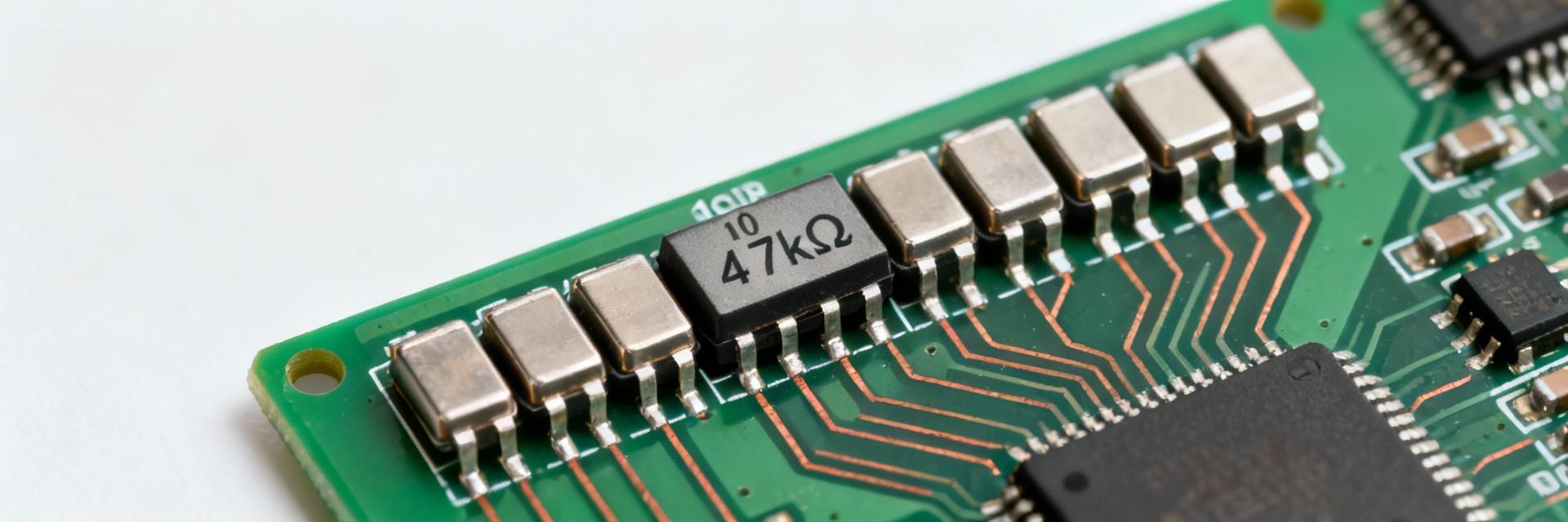
Core identity and typical package
A 9-element bussed SIP resistor network ties one end of nine identical resistors to a single common pin, with the other ends routed to individual pins, yielding ten total pins on a standard SIP. Typical mounting is low-profile through-hole for robust lead retention; pitch is standard 2.54 mm (0.100") with a compact body height suited to constrained PCBs. Designers choose a bussed resistor network for consistent pull-up/pull-down behavior and simplified routing compared to discrete parts.
Short spec summary table
Quick facts for fast reference; each line is a headline spec for scan reading.
| Resistance value | 4.7 kΩ per element |
| Tolerance | ±2% |
| Power per element | ~200 mW (continuous rating) |
| TCR | 100 ppm/°C |
| Temperature range | ≈ −55 °C to +125 °C |
| Pins / resistors | 10 pins / 9 resistors (bussed) |
| Technology | Thick-film |
Full electrical specification breakdown (data analysis)
Resistance value, tolerance and arrangement
The nominal 4.7 kΩ value with ±2% tolerance gives a worst-case range of approximately 4,606 Ω to 4,794 Ω per element (4,700 × (1 ± 0.02)). In bussed arrays the common node ties one end of each resistor together, making them ideal for uniform pull-ups or pull-downs on parallel inputs. Example: a microcontroller input expecting a threshold at 1.4 V with a 10 kΩ pull-up network will see predictable biasing when each element remains within the stated tolerance band.
Voltage, power and derating behavior
With P ≈ 0.2 W per element, the nominal maximum steady RMS voltage across a 4.7 kΩ element is Vmax ≈ sqrt(P×R) ≈ sqrt(0.2×4,700) ≈ 30.7 V (use Ractual for precise per-lot numbers). Continuous vs peak: continuous rating is conservative; short-duration pulses may exceed it if thermal time constants are respected. For elevated ambient conditions apply linear or vendor-supplied derating—example guideline: limit element dissipation to 60–80% of nameplate at +85 °C. [confirm max element voltage per datasheet]
Thermal performance, TCR and reliability (data analysis)
Temperature coefficient of resistance (TCR) and stability
Key specs to watch: TCR = 100 ppm/°C means a fractional change of 0.0001 per °C. Over a −40 °C to +85 °C span (ΔT = 125 °C) expect about a 1.25% change in resistance, i.e., ~59 Ω on a 4.7 kΩ element. For precision ADC reference dividers or matched networks this shift is material; consider lower-TCR alternatives or temperature compensation when measurement error budgets are tight. Thick-film technology also exhibits modest long-term drift—specify lot stability tests for critical runs.
Thermal limits, derating and expected lifetime
Rated operating range near −55 °C to +125 °C implies the package tolerates wide ambient swings, but internal element temperature rises under dissipation reduce margin. Thermal coupling among elements concentrates heat inside the package, lowering per-element allowable power vs isolated resistors. Reliability checks should include thermal cycling and humidity tests; incoming lot tests should exercise power-soak at elevated ambient to screen weak units and qualify lifetime under expected board copper area and airflow conditions.
Design-in guide — footprint, assembly and test procedures (method guide)
PCB footprint, mechanical placement and soldering
Use a 2.54 mm pin pitch footprint with pad drills sized for through-hole leads; recommended annular pad diameter ~1.2–1.5 mm and solder fillet clearance on both sides. Keep a small keepout around the body for thermal relief and mark orientation on silkscreen at the common pin. Through-hole leads suit wave or hand solder; allow mechanical strain relief in silkscreen or pick-and-place tooling and avoid tight traces under the body that impede heat dissipation.
Electrical test procedures and validation on the bench
Test recipe: measure each element at room temperature with a precision DMM, verify within ±2%; check bus continuity by measuring resistance between common pin and each node (expected ~Rvalue). Power-soak test: apply 0.2 W to a single element while monitoring temperature rise; confirm no drift beyond tolerance after soak. For derating validation, run thermal-chamber sweeps at expected ambient extremes and verify resistance vs temperature. Pass/fail: R within tolerance at 25 °C and no open/short after power soak.
Typical applications, selection checklist & alternatives (case + action)
Typical use-cases and real-world examples
Common applications include input-line pull-ups/pull-downs for keyed buses, resistor banks for LED arrays where identical values simplify drive, and mapping resistors for selector networks. A bussed 9-element 4.7 kΩ, ±2% device is a fit when identical biasing is required across many lines and board area or placement simplicity matters. Caveats: precision thresholds or higher per-channel power call for discrete or higher-spec arrays.
Selection and procurement checklist before production
Checklist: confirm nominal value & ±2% tolerance, validate power per element and a derating plan for ambient/PCB conditions, verify TCR and operating temperature range, confirm package pinout and footprint compatibility, define lot testing (IR, power-soak, thermal cycling), ensure RoHS/lead-free requirements and qualify alternatives for supply risk. Incorporate acceptance criteria into incoming inspection procedures to avoid field failures.
Summary
- The 4310R-101-472 provides nine 4.7 kΩ bussed resistors in a 10-pin SIP package, suitable for compact pull-up/pull-down arrays and reducing discrete placement complexity.
- Evaluate power derating carefully: nominal 200 mW per element yields ~30.7 V theoretical across a 4.7 kΩ element, but ambient and package coupling reduce continuous allowance.
- TCR = 100 ppm/°C implies ~1.25% change across a −40 to +85 °C span; assess impact on ADC/reference circuits and consider lower-TCR parts for precision needs.
- Use the provided PCB, soldering and test recipes—DMM checks, power-soak and thermal-chamber sweeps—to qualify incoming lots before production.
FAQ
How does tolerance and TCR affect circuit thresholds for the 4310R-101-472?
Tolerance ±2% sets the static resistance band; combined with a 100 ppm/°C TCR, temperature swings introduce additional percent-level shifts. For threshold-sensitive inputs, calculate worst-case using Rmin/Rmax plus TCR-induced delta across operating ΔT and confirm thresholds remain valid under those extremes.
What voltage can be safely applied across one element?
Use Vmax ≈ sqrt(P×R) with P as the continuous power rating. For 0.2 W and 4.7 kΩ, Vmax ≈ 30.7 V; verify with the datasheet and apply derating for elevated ambient. If the datasheet does not list maximum element voltage explicitly, include “[confirm max element voltage per datasheet]” in your procurement checks.
What incoming tests should manufacturing perform on these resistor networks?
Minimum incoming tests: room-temperature resistance sweep of all nine elements (±2% pass), bus continuity check, and sample power-soak/thermal cycling to validate derating assumptions. Add humidity and mechanical stress tests for harsher environments and document acceptance criteria in the purchase order.
- Technical Features of PMIC DC-DC Switching Regulator TPS54202DDCR
- STM32F030K6T6: A High-Performance Core Component for Embedded Systems
- APT50GH120B Datasheet Deep Dive: Specs, Ratings & Curves
- SI3402-B-GMR PoE PD Controller: Market & Specs Report
- SI3402-B-GMR Benchmarks: Real PoE Performance Insights
- EFM8BB21F16G Full Datasheet & Pinout: Specs Summary
- CP2102N-A02-GQFN20R Pinout & Footprint: Quick Data Guide
- SI53307-B-GMR Datasheet & CAD Models: Quick Specs Checklist
- SI53361-B-GMR: Latest Specs, Stock Levels & Price Guide
- SI53340-B-GM: Deep Performance Report & Key Metrics
-
 EXB-V4V120JVPanasonic Electronic ComponentsRES ARRAY 2 RES 12 OHM 0606
 -
 EXB-V4V473JVPanasonic Electronic ComponentsRES ARRAY 2 RES 47K OHM 0606
 -
 EXB-V4V823JVPanasonic Electronic ComponentsRES ARRAY 2 RES 82K OHM 0606
 -
 EXB-V4V151JVPanasonic Electronic ComponentsRES ARRAY 2 RES 150 OHM 0606
 -
 EXB-V4V181JVPanasonic Electronic ComponentsRES ARRAY 2 RES 180 OHM 0606
 -
 EXB-V4V331JVPanasonic Electronic ComponentsRES ARRAY 2 RES 330 OHM 0606
 -
 EXB-V4V152JVPanasonic Electronic ComponentsRES ARRAY 2 RES 1.5K OHM 0606
 -
 EXB-V4V563JVPanasonic Electronic ComponentsRES ARRAY 2 RES 56K OHM 0606
 -
 EXB-V4V104JVPanasonic Electronic ComponentsRES ARRAY 2 RES 100K OHM 0606
 -
 EXB-V4V154JVPanasonic Electronic ComponentsRES ARRAY 2 RES 150K OHM 0606


