-
- Contact Us
- Privacy Policy
- term and condition
- Cookies policy
CMSG120N013MDG Datasheet Deep Dive: Key Specs & Ratings
The following analysis unpacks the datasheet headline ratings and practical limits for a 1200 V, high-current hybrid power module. Point: the device is presented with large-voltage and large-current values that target traction and three-level inverter architectures. Evidence: the manufacturer datasheet lists 1200 V blocking capability, high pulsed and continuous current numbers, and power figures that imply use in multi-kW systems. Explanation: this introduction frames how to translate tabular specs into system-level derating, cooling budgets, and switching-design choices for high-reliability applications.
Introduction
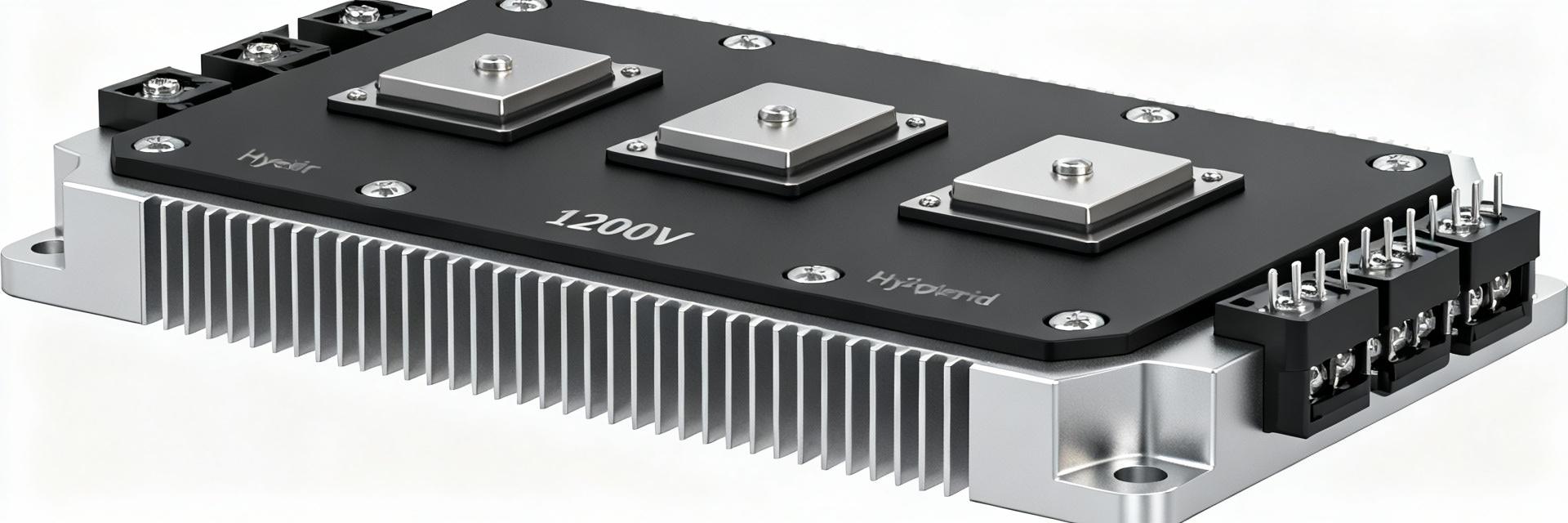
Point: a concise, data-driven hook clarifies why engineers consider this module for high-voltage conversion. Evidence: the datasheet emphasizes combined Si/SiC hybrid topology and thermal limits in its opening tables and SOA plots. Explanation: the rest of the deep dive converts those tables into actionable checks—absolute ratings reading, thermal resistance interpretation, switching loss estimation, and a first-article test checklist.
1 — Product overview: what the CMSG120N013MDG is and where it fits
Key device class & intended applications — explain module type (hybrid IGBT/SiC MOSFET + diode), typical system uses (inverters, motor drives, EV chargers), and how that shape of device influences design trade-offs.
Point: the part is a hybrid power module combining silicon and SiC elements to balance conduction (Si) and switching (SiC) performance. Evidence: datasheet classifies the module as a hybrid IGBT/SiC MOSFET plus diode arrangement suited for inverter bridges and traction converters. Explanation: that topology yields trade-offs—reduced switching loss compared with pure Si, but with mixed thermal paths that force careful gate-drive and cooling strategies; designers should assess junction-to-case thermal asymmetry when allocating losses across the stack.
Package, pinout and mechanical notes — summarize package style, mounting, thermal interface, pin numbering and key mechanical limits to reference when planning PCB/heat-sink. Point to which datasheet figures to screenshot.
Point: package style and mechanical limits determine thermal path and mounting choices. Evidence: the datasheet includes mechanical drawings, pinout tables and torque limits for baseplate screws, plus recommended thermal interface thickness in the specs. Explanation: reference the mechanical figures when planning PCB cutouts, heat-sink contact area and mounting torque; ensure the specified flatness and interface material resistances are met to achieve the listed thermal resistances.
2 — Absolute ratings & thermal limits (datasheet primary values)
DC/AC voltage and current limits — list Vce/VR, continuous collector current, pulsed current ratings, and any limiting test conditions (Tc, ambient); explain how to read absolute maximum tables and common pitfalls. (Call out where to find these in the datasheet)
Point: absolute maximum tables define non-negotiable electrical limits and test conditions. Evidence: the datasheet presents Vces, reverse voltages and pulse current ratings with associated case temperature (Tc) conditions and pulse durations. Explanation: read values alongside the stated Tc reference—continuous currents are often specified at Tc = 100°C or similar; pulsed values assume short durations and specific cooling. Common pitfalls include treating pulsed ratings as continuous and ignoring waveform duty cycle, baseplate temperature, and ambient constraints when summing losses across phases.
Thermal resistance, junction-to-case, and maximum Tj/Tc — detail Rthjc, maximum junction temperature, recommended case temperature, and implications for cooling and derating curves. Provide a quick derating example. (Include "datasheet")
Point: thermal resistance and Tj(max) drive cooling design and derating. Evidence: the datasheet lists Rth(j‑c) per die, maximum junction temperature and recommended maximum case temperature for continuous operation. Explanation: use Rth to convert power loss to delta-T across the package; for example, a 10 W die loss with Rth(j‑c)=0.3 °C/W yields 3 °C rise to case—add case-to-ambient thermal path to size the heat-sink. Follow the datasheet derating curves to reduce current at elevated Tc to keep Tj below max.
| Parameter | Typical value (example) | Design implication |
|---|---|---|
| Rth(j‑c) | 0.2–0.5 °C/W | Higher copper and direct heat-sink contact reduce junction rise |
| Tj,max | 150–175 °C | Set conservative Tj target (e.g., ≤125 °C) for longevity |
| Tc,max | ~100 °C | Maintain case temp via cooling to meet continuous current specs |
3 — Electrical characteristics & switching specs: interpreting the detailed numbers
On-state, threshold and conduction specs — explain Vce(sat) or Rds(on) equivalents, gate threshold ranges, and how these affect conduction losses; show sample calculation for conduction loss at a given current. (Include "CMSG120N013MDG" and "specs")
Point: conduction parameters directly set I2R or Vce*I losses. Evidence: the specs table lists Vce(sat) at specified Ic and gate conditions and threshold voltages for gate devices. Explanation: take Vce(sat)=1.2 V at 100 A as an example (datasheet sample): conduction loss = Vce(sat) × I = 1.2 V × 100 A = 120 W per device; for PWM duty control, scale by duty cycle. Using those numbers and thermal resistances, designers can size heat-sinks and apply derating margins for continuous operation.
Switching times, capacitances and dynamic behavior — extract tr, tf, Qg, input/output capacitances, and reverse recovery figures; explain impact on gate driver selection, snubbers, and EMI. Provide recommended test waveforms to validate switching behavior.
Point: dynamic specs govern driver sizing and snubber design. Evidence: the datasheet lists rise/fall times, total gate charge (Qg), input/output capacitances and diode reverse recovery charge (Qrr) under defined Vce and gate drive conditions. Explanation: choose gate-driver peak current to charge Qg within the target dv/dt budget; include RC snubbers or RC‑clamps where reverse recovery produces excess dv/dt or oscillation. Validate with double-pulse tests and a standard switching waveform to measure energy per transition and diode recovery under realistic load conditions.
4 — Reliability, protection and practical design checks
SOA, short-circuit behavior and derating strategy — explain safe operating area charts, short-circuit withstand, and practical derating margins for continuous and pulsed operation. Give checklist items to verify during design.
Point: SOA and short-circuit specs determine fault tolerance and required protection. Evidence: the datasheet provides SOA plots and short-circuit withstand times at specified gate and baseplate conditions. Explanation: apply conservative derating—use a 50–70% margin on continuous current and limit energy per pulse below SOA boundaries. Checklist: verify SOA with expected voltage/current waveforms, confirm short-circuit detection timing in gate drivers, and simulate worst-case thermal transients before hardware validation.
Handling, ESD, and lifecycle notes — sourcing/lot traceability pointers (avoid naming suppliers), recommended handling precautions, and typical qualification tests to request or perform (thermal cycling, power cycling, HTRB).
Point: handling and qualification ensure long-term reliability. Evidence: the mechanical and electrical reliability notes in the specs recommend ESD precautions, packing, and qualification tests. Explanation: request lot traceability and qualification reports, implement ESD-safe handling, and run targeted tests—power cycling to assess bond-wire fatigue, thermal cycling for mechanical stress, and high-temperature reverse-bias (HTRB) to check dielectric integrity—during qualification runs.
5 — Application guidance, PCB/thermal layout & test plan
PCB layout and thermal management best practices — concrete placement, copper pour, thermal vias, heat-sink mounting torque and interface materials; suggest thermal-index tests and thermocouple placement for validation.
Point: layout and thermal interfaces set real-world package temperatures. Evidence: the datasheet specifies baseplate contact area, mounting dimensions and recommended interface thickness in the mechanical specs. Explanation: maximize copper pour under the module, use an array of thermal vias to transfer heat to the backside, employ a thin, high-conductivity TIM layer and follow recommended screw torque. Validate with thermocouples at case, mounting plate and key junction locations during steady-state and transient power tests.
Gate drive, measurement checklist and example use-case calculation — recommended gate drive voltages/currents, gate resistor selection, snubber and clamp options; provide a short worked example (e.g., loss and heat-sink sizing for a 100 kW inverter leg). Include a concise test plan for first-article validation. (Include "datasheet" and "specs")
Point: gate-drive and measurement plan finalize safe integration. Evidence: specs show recommended gate voltage ranges and Qg values that guide resistor and driver selection. Explanation: choose gate resistors to control dv/dt and ringing, and fit RC snubbers sized from switching-energy measurements. Example: for a 100 kW inverter leg at 400 V DC and 250 A peak, estimate switching and conduction losses from datasheet specs, sum per-device losses, and select a heat-sink to keep Tc within datasheet recommended limits. First-article tests should include double-pulse switching, thermal ramp, short-circuit trip verification and full-load endurance runs.
Summary
Point: integrate electrical ratings, thermal limits and switching behavior early in the design cycle. Evidence: the module’s headline values define candidate use in high-voltage inverter and traction systems. Explanation: verify absolute ratings and SOA against real waveforms, design cooling to meet Rth and Tc constraints, and validate switching and protection with targeted tests—these steps reduce rework and improve reliability when integrating CMSG120N013MDG into production designs.
Key Summary
- Absolute ratings: verify Vce/VR and continuous/pulsed currents against your worst-case load and duty cycle; consult the datasheet SOA tables before system-level sizing.
- Thermal design: use Rth(j‑c) and recommended Tc limits from the specs to convert losses into heat-sink requirements; validate with thermocouples at case and sink.
- Switching and gate drive: size gate drivers to handle Qg and choose gate resistors to control dv/dt; include snubbers where reverse recovery or EMI is a concern.
- Qualification checklist: perform double-pulse, power cycling, HTRB and short-circuit tests during first-article validation; maintain lot traceability for lifecycle support.
FAQ
What are the key datasheet limits I should check first?
Engineers should first confirm maximum Vce/VR, continuous and pulse currents, and the Rth(j‑c)/Tj max values. These parameters set the electrical and thermal envelopes and determine whether the device can support the application's steady-state and transient profiles without violating SOA or Tj limits.
How do I use the datasheet to size a heat-sink?
Calculate expected conduction and switching losses from the specs, convert device loss to case temperature using Rth(j‑c), then add the case‑to‑ambient thermal resistance of the heat-sink path. Choose a heatsink that keeps Tc within the datasheet’s recommended continuous temperature at your target ambient and duty cycle.
What tests should be in the first-article validation plan?
Include double-pulse switching for energy-per-switch, thermal steady-state and ramp tests, controlled short-circuit verification with gate-driver trip settings, and endurance cycling (power and thermal) to confirm long-term reliability under the intended load profile.
- Technical Features of PMIC DC-DC Switching Regulator TPS54202DDCR
- STM32F030K6T6: A High-Performance Core Component for Embedded Systems
- APT50GH120B Datasheet Deep Dive: Specs, Ratings & Curves
- SI3402-B-GMR PoE PD Controller: Market & Specs Report
- SI3402-B-GMR Benchmarks: Real PoE Performance Insights
- EFM8BB21F16G Full Datasheet & Pinout: Specs Summary
- CP2102N-A02-GQFN20R Pinout & Footprint: Quick Data Guide
- SI53307-B-GMR Datasheet & CAD Models: Quick Specs Checklist
- SI53361-B-GMR: Latest Specs, Stock Levels & Price Guide
- SI53340-B-GM: Deep Performance Report & Key Metrics
-
 EXB-V4V120JVPanasonic Electronic ComponentsRES ARRAY 2 RES 12 OHM 0606
 -
 EXB-V4V473JVPanasonic Electronic ComponentsRES ARRAY 2 RES 47K OHM 0606
 -
 EXB-V4V823JVPanasonic Electronic ComponentsRES ARRAY 2 RES 82K OHM 0606
 -
 EXB-V4V151JVPanasonic Electronic ComponentsRES ARRAY 2 RES 150 OHM 0606
 -
 EXB-V4V181JVPanasonic Electronic ComponentsRES ARRAY 2 RES 180 OHM 0606
 -
 EXB-V4V331JVPanasonic Electronic ComponentsRES ARRAY 2 RES 330 OHM 0606
 -
 EXB-V4V152JVPanasonic Electronic ComponentsRES ARRAY 2 RES 1.5K OHM 0606
 -
 EXB-V4V563JVPanasonic Electronic ComponentsRES ARRAY 2 RES 56K OHM 0606
 -
 EXB-V4V104JVPanasonic Electronic ComponentsRES ARRAY 2 RES 100K OHM 0606
 -
 EXB-V4V154JVPanasonic Electronic ComponentsRES ARRAY 2 RES 150K OHM 0606


