-
- Contact Us
- Privacy Policy
- term and condition
- Cookies policy
GTSM20N065 650V IGBT Datasheet: Key Specs & Metrics
The GTSM20N065 650V IGBT datasheet is summarized here to give engineers and buyers a focused, actionable distillation of the device’s key specs and design checks. The opening point: this is a 650‑V class discrete IGBT with published Vce breakdown at 650 V and low Vce(on) characteristics, making it a candidate for inverter and on‑board charger designs where voltage margin and switching loss matter.
1 — Product overview & absolute ratings (background)
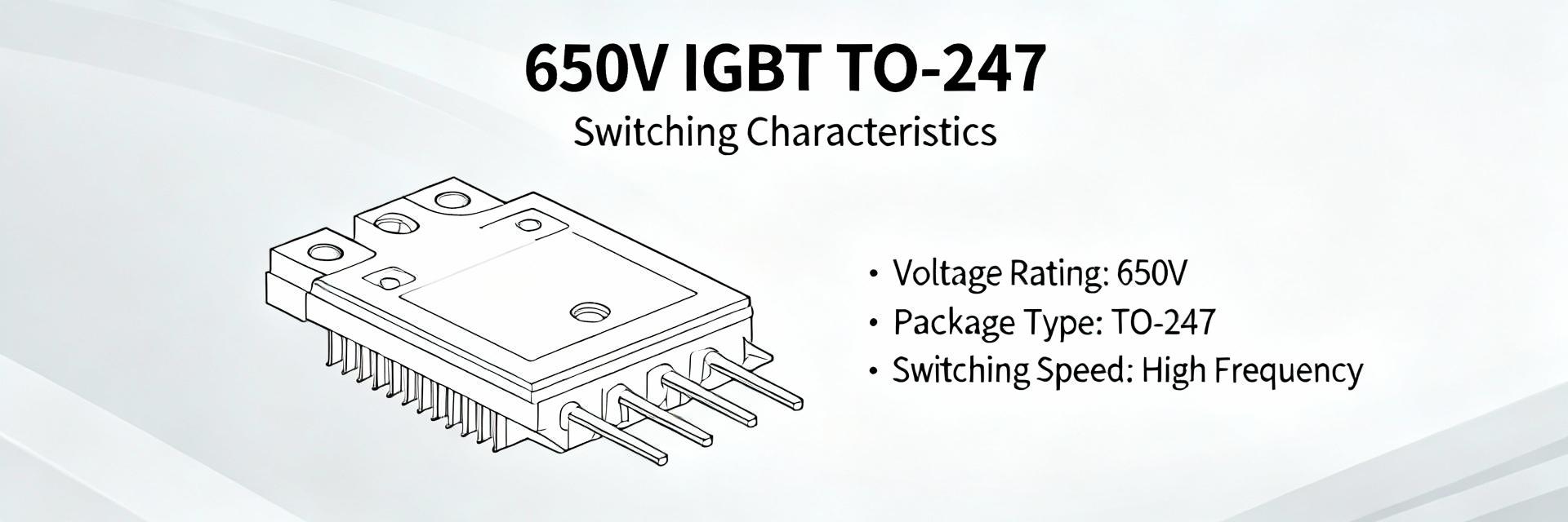
— Package, pinout & variant IDs
Point: The device is supplied in a single‑device power package (TO‑247‑like power package). Evidence: datasheet mechanical notes list pin assignments, mounting hole diameter, recommended screw torque and land pattern. Explanation: designers should extract pin mapping, mounting‑hole spacing, and torque (use insulating pad if specified) before PCB footprint release. Table: quick mechanical specs for layout reference.
| Item | Typical |
|---|---|
| Package | TO‑247 style power package |
| Mount hole | Ø ~3.5–4.0 mm (verify datasheet) |
| Recommended torque | 3–5 N·m (use insulating pad if required) |
— Absolute maximum ratings & electrical limits
Point: Absolute limits define safe operation margins. Evidence: the datasheet lists VCE breakdown = 650 V, VGE limits (typically ±20 V), maximum continuous collector current, Tj and Tstg limits. Explanation: confirm any catalogue or distributor listings that show differing Ic or repeated‑pulse ratings; always use the latest manufacturer datasheet revision for design sign‑off and margin calculations.
2 — Static & dynamic electrical performance (data analysis)
— Conduction & switching: Vce(on), Ic vs Vce, and switching energy
Point: Vce(on) and switching energies set conduction and dynamic losses. Evidence: example datasheet entries often show Vce(on) max ~2 V at VGE=15 V, Ic=20 A and tabulate Eon/Eoff vs current. Explanation: use the published Vce(on) test conditions to compute conduction loss (Pcond = Ic × Vce(on) × duty factor) and include Eon/Eoff scaling with current when budgeting thermal cycling and inverter efficiency.
— Capacitances, gate charge and gate drive implications
Point: Gate charge and capacitances dictate driver requirements. Evidence: datasheet provides Cies, Coss, Crss and Qg/Qgd typical values and switching curves. Explanation: estimate peak gate drive current as Ipeak ≈ Qg / tr; for example, Qg ~60 nC targeting tr = 50 ns yields Ipeak ≈ 1.2 A. Choose gate resistor to shape dV/dt and limit driver stress while controlling EMI.
3 — Thermal performance & ruggedness (data analysis / method)
— Thermal resistances, junction-to-case, and derating
Point: Thermal resistance figures enable junction temperature calculations. Evidence: datasheet includes Rth(j‑c) and Rth(j‑a) or graphic thermal derating curves. Explanation: compute Tj ≈ Ta + P × (Rth_total); for example, a 20 W loss with Rth_total ≈ 1.5 K/W raises junction ≈30 °C above ambient. Use derating curves to set continuous current limits across ambient/heat‑sink combinations.
— Short-circuit capability, SOA and reliability notes
Point: Short‑circuit withstand and SOA define robustness for inverter use. Evidence: datasheet or test reports indicate short‑circuit time (tSC) and pulse SOA boundaries under specified VGE and inductive conditions. Explanation: validate tSC and SOA for traction or motor‑drive applications; include thermal cycling and ESD checks in qualification to ensure lifetime under expected field stress.
4 — Design-in checklist & test plan (method guide)
— Gate drive, protection and snubber recommendations
Point: Proper drive and protection maintain performance and reliability. Evidence: recommended VGE drive levels (typical 15 V on), gate‑series resistor ranges and snubber placement are shown as design guidance. Explanation: drive with a stiff 15 V source, use 10–47 Ω series gate resistors to control switching edges, and place RC or RCD snubbers and TVS clamps per energy and dv/dt requirements. Verify with oscilloscope under load to refine values.
— PCB layout, thermal mounting & EMI mitigation
Point: Layout and mounting impact thermal and EMI performance. Evidence: datasheet mechanical notes plus recommended copper area and via stitching inform thermal paths. Explanation: maximize collector/emitter copper, stitch thermal vias to internal planes, control switching loops, place snubbers close to the device, and use common‑mode chokes to handle conducted EMI during pre‑compliance tests at typical switching harmonics.
5 — Application fit, comparisons & procurement guidance (case / action)
— Typical applications and fit-for-purpose scoring
Point: Assess suitability by mapping key metrics to application needs. Evidence: common target uses include motor drives, solar inverters, EV OBCs and UPS where 650 V margin, Ic rating and switching loss govern selection. Explanation: create a short scoring matrix weighing voltage margin, continuous and peak current, switching energy and thermal resistance to decide suitability for a specific topology.
— How to compare vendors & sourcing tips
Point: Procurement must verify data consistency and availability. Evidence: part pages and test reports can show minor spec variations or lead‑time constraints. Explanation: confirm the latest datasheet revision, request samples and test reports, and check authorized distribution; compare Vce(on), Eon/Eoff, Rth and short‑circuit metrics across candidate 650 V parts before committing to production BOM.
Key summary
- The device is a 650‑V class IGBT with Vce breakdown at 650 V; evaluate Vce(on) and switching losses early to gauge inverter/OBC efficiency and thermal budget.
- Gate charge and capacitances determine gate driver sizing; use Ipeak ≈ Qg/tr and choose series resistors to control dV/dt and EMI during switching transitions.
- Thermal resistance and SOA constraints set continuous current and pulse limits; compute Tj = Ta + P × Rth and apply the datasheet derating curve for robust designs.
Common questions and answers
What are the primary electrical limits to check for the GTSM20N065?
Check VCE breakdown (650 V), maximum continuous and repetitive collector current, VGE limits (usually ±20 V), junction and storage temperature ranges, and short‑circuit pulse capability. Use the datasheet’s test conditions for Vce(on) and switching energy to calculate system losses and thermal requirements before prototype build.
How should a gate driver be sized for this 650V IGBT?
Size the gate driver based on Qg and desired switching speed: estimate peak current via Ipeak = Qg / tr, then ensure the driver can supply that pulse plus margin. Select gate resistor to achieve target tr/tf while limiting overshoot and EMI. Include a clamp or gate zener if VGE max is tight.
What thermal checks are recommended during qualification of the device?
Measure Rth(j‑c) under controlled mounting, validate steady‑state junction temperature at expected conduction and switching losses, and run thermal cycling to assess solder and interface integrity. Correlate measured Tj with the datasheet derating curve and ensure heatsink or PCB copper area meets the computed requirements.
Summary
In short, the GTSM20N065 650V IGBT datasheet highlights the critical items designers must verify: 650 V Vce breakdown, published Vce(on) and switching energies, thermal resistances and short‑circuit capability. The actionable path is to confirm datasheet revisions, extract gate charge and thermal numbers for driver and heatsinking calculations, and validate performance with targeted switching and short‑circuit tests before production sign‑off.
- Technical Features of PMIC DC-DC Switching Regulator TPS54202DDCR
- STM32F030K6T6: A High-Performance Core Component for Embedded Systems
- APT50GH120B Datasheet Deep Dive: Specs, Ratings & Curves
- SI3402-B-GMR PoE PD Controller: Market & Specs Report
- SI3402-B-GMR Benchmarks: Real PoE Performance Insights
- EFM8BB21F16G Full Datasheet & Pinout: Specs Summary
- CP2102N-A02-GQFN20R Pinout & Footprint: Quick Data Guide
- SI53307-B-GMR Datasheet & CAD Models: Quick Specs Checklist
- SI53361-B-GMR: Latest Specs, Stock Levels & Price Guide
- SI53340-B-GM: Deep Performance Report & Key Metrics
-
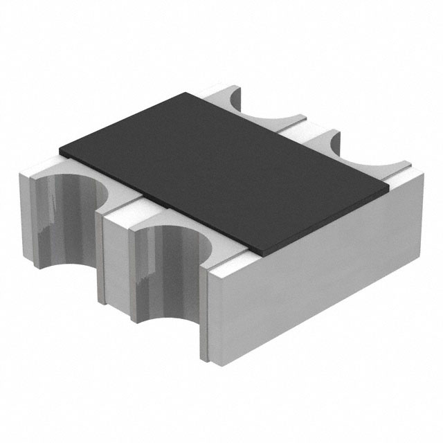 EXB-V4V120JVPanasonic Electronic ComponentsRES ARRAY 2 RES 12 OHM 0606
 -
 EXB-V4V473JVPanasonic Electronic ComponentsRES ARRAY 2 RES 47K OHM 0606
 -
 EXB-V4V823JVPanasonic Electronic ComponentsRES ARRAY 2 RES 82K OHM 0606
 -
 EXB-V4V151JVPanasonic Electronic ComponentsRES ARRAY 2 RES 150 OHM 0606
 -
 EXB-V4V181JVPanasonic Electronic ComponentsRES ARRAY 2 RES 180 OHM 0606
 -
 EXB-V4V331JVPanasonic Electronic ComponentsRES ARRAY 2 RES 330 OHM 0606
 -
 EXB-V4V152JVPanasonic Electronic ComponentsRES ARRAY 2 RES 1.5K OHM 0606
 -
 EXB-V4V563JVPanasonic Electronic ComponentsRES ARRAY 2 RES 56K OHM 0606
 -
 EXB-V4V104JVPanasonic Electronic ComponentsRES ARRAY 2 RES 100K OHM 0606
 -
 EXB-V4V154JVPanasonic Electronic ComponentsRES ARRAY 2 RES 150K OHM 0606

