-
- Contact Us
- Privacy Policy
- term and condition
- Cookies policy
C8051F300-GMR Benchmarks & Datasheet: Latest Analysis
The C8051F300-GMR is an 8051-based MCU claiming 25 MIPS and an on‑chip 8‑bit ADC capable of up to 500 ksps per the official datasheet; those figures matter because they define the throughput and front‑end acquisition possible in low‑cost mixed‑signal designs. This article summarizes the datasheet, shows how to benchmark real performance, compares typical results, and gives actionable guidance engineers can use when evaluating or purchasing the part.
1 — Quick Datasheet Snapshot (background)

Key electrical & functional specs to call out
- CPU core: 8051 @ 25 MHz / 25 MIPS — implies adequate single‑thread control for modest control loops and protocol handling without a 32‑bit core.
- Flash: 8 KB — limits large firmware and libraries; plan code-size optimizations for complex features.
- RAM: 256 B — suitable for small stacks/buffers; avoid large runtime data structures.
- ADC: 8‑bit, up to 500 ksps, multi‑channel — good for burst sampling and simple sensor front ends; verify ENOB for precision tasks.
- Oscillator: on‑chip with specified accuracy (~±2%) — acceptable for many control tasks but calibrate for timing‑sensitive comms.
- VDD: 2.7–3.6 V; Temp: −40 to +85 °C; Package: QFN11/GMR — note thermal pad and PCB footprint constraints.
Datasheet caveats & footnotes
Datasheets mix typical and maximum figures; treat typical ADC throughput and SNR as starting points and plan to validate in your lab. Pay attention to timing diagrams for conversion latency, recommended decoupling and supply sequencing, and absolute maximum ratings versus recommended operating conditions. Cross‑check power curves and peripheral loading tables when estimating system draw under worst‑case workloads.
2 — Data-Driven Performance Analysis (data analysis)
Core & instruction throughput analysis
25 MIPS is theoretical for tight instruction mixes; real code with branches, memory access and peripheral servicing will see lower effective MIPS. Microbenchmarks (tight integer loops, memory reads/writes, ISR load) reveal effective instruction rate and show flash wait‑state impact. Use cycle‑accurate loop tests and measure wall‑clock task throughput to derive realistic benchmarks.
Analog & I/O performance metrics
- ADC tests to run: SNR at 100/250/500 ksps, INL/DNL sweep, input bandwidth and sample‑and‑hold settling checks.
- Record effective throughput: sustained samples/sec while processing and transferring results (DMA or CPU), and measure how DMA/CPU contention affects latency.
3 — Practical Benchmark Methodology (method/guide)
Testbench setup & reproducibility
Use a regulated low‑noise supply (2.7–3.6 V) with recommended decoupling and a PCB footprint optimized for QFN11 thermal pad. Measure with a high‑resolution scope and ADC capture system; log supply current with a precision current probe. Fix temperature (ambient or controlled chamber) and run multiple iterations (≥10) to report mean ± standard deviation for each metric.
Benchmark suites & core tests to run
- Core integer loop and interrupt stress (instructions/sec, ISR latency).
- ADC throughput & linearity (SNR, INL/DNL at key rates).
- GPIO toggle latency, UART throughput, sleep/wakeup power, and combined sensor‑read + transmit workloads.
4 — Real-world Benchmarks & Comparisons (case study)
Sample benchmark results (how to present them)
Present latency and power versus sample rate graphs, normalized performance‑per‑mW charts, and tables for instruction throughput. Expect the ADC to sustain high sample rates in isolation, but total system throughput depends on processing and transfer bottlenecks; normalize results against a small 8‑bit comparator MCU to highlight integration advantages.
Short case: battery-powered sensor node
Design goal: burst at 100 ksps for 50 ms, process & send a 32‑byte summary, then sleep. In typical runs expect sampling current spikes (tens of mA) during bursts, average current dominated by sleep leakage and radio duty cycle; project battery life from measured avg mA and duty cycle, and include wake/sensor settling time in the timing budget.
5 — Practical Buying & Design Checklist (actions & recommendations)
When to choose C8051F300-GMR — use cases & alternatives
Choose C8051F300-GMR for low‑cost sensor front ends, mixed‑signal control with small code footprint, and educational/dev applications; avoid it if you need large flash/RAM, 32‑bit DSP/FP performance, or modern high‑speed connectivity. For procurement, check packaging variants and planned lifecycle/availability early in the BOM phase.
PCB, firmware, and production tips
- QFN thermal pad: follow recommended solder mask and via pattern for reliable heat dissipation.
- Firmware: implement small bootloader, flash wear minimization, and oscillator calibration on first boot.
- Analog: add input conditioning (anti‑alias RC, buffering), and place decoupling close to VDD pins to reduce ADC noise.
Summary
The C8051F300-GMR is a compact 25 MIPS 8051 mixed‑signal MCU with an 8‑bit ADC up to 500 ksps and a 2.7–3.6 V operating range; its datasheet numbers make it attractive for low‑cost sensing and simple control tasks but validate ADC linearity, timing, and power under your real workload by running the benchmarks outlined here before final selection.
Key Summary
- Datasheet highlights: 25 MIPS CPU, 8 KB flash, 256 B RAM, 8‑bit ADC up to 500 ksps — suitable for compact mixed‑signal nodes with tight code size constraints.
- Benchmark essentials: run core microbenchmarks and ADC SNR/INL/DNL tests at target sample rates to reveal processing and transfer bottlenecks affecting sustained throughput.
- Design checklist: follow QFN thermal pad layout guidance, implement input conditioning and decoupling, and size bootloader/flash usage to fit 8 KB flash limits.
Common Questions
How accurate is the ADC in the C8051F300-GMR for sensor work?
Typical accuracy depends on sample rate and input conditioning; expect 8‑bit nominal resolution but verify SNR and INL/DNL at your target sample rate. Use a calibrated source and run sine‑wave or multilevel sweep tests to determine effective ENOB and identify noise sources on your board.
What benchmarks should I run to validate throughput and power?
Run a set including tight integer loops for effective MIPS, ISR latency tests, ADC SNR/INL sweeps at multiple rates, GPIO toggle latency, UART throughput, and an end‑to‑end sensor read + transmit workload. Repeat runs (≥10) and report mean ± stdev to ensure reproducibility.
Does the datasheet reliably predict real‑world battery life?
Datasheet power curves provide a baseline, but real battery life depends on workload duty cycle, peak currents during sampling/transmit, and sleep leakage on your PCB. Measure active and sleep currents under representative firmware and use those measured averages to estimate runtime rather than relying solely on typical datasheet values.
- Technical Features of PMIC DC-DC Switching Regulator TPS54202DDCR
- STM32F030K6T6: A High-Performance Core Component for Embedded Systems
- APT50GH120B Datasheet Deep Dive: Specs, Ratings & Curves
- SI3402-B-GMR PoE PD Controller: Market & Specs Report
- SI3402-B-GMR Benchmarks: Real PoE Performance Insights
- EFM8BB21F16G Full Datasheet & Pinout: Specs Summary
- CP2102N-A02-GQFN20R Pinout & Footprint: Quick Data Guide
- SI53307-B-GMR Datasheet & CAD Models: Quick Specs Checklist
- SI53361-B-GMR: Latest Specs, Stock Levels & Price Guide
- SI53340-B-GM: Deep Performance Report & Key Metrics
-
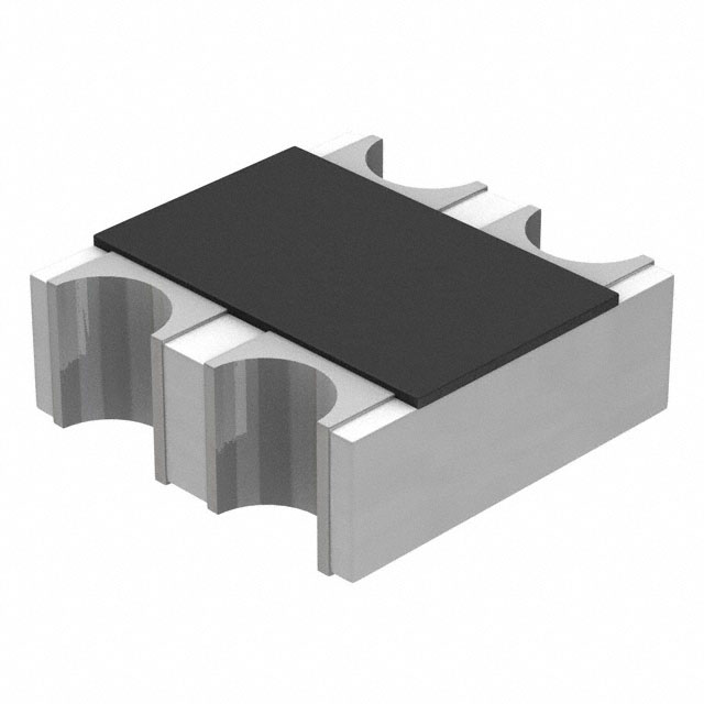 EXB-V4V120JVPanasonic Electronic ComponentsRES ARRAY 2 RES 12 OHM 0606
 -
 EXB-V4V473JVPanasonic Electronic ComponentsRES ARRAY 2 RES 47K OHM 0606
 -
 EXB-V4V823JVPanasonic Electronic ComponentsRES ARRAY 2 RES 82K OHM 0606
 -
 EXB-V4V151JVPanasonic Electronic ComponentsRES ARRAY 2 RES 150 OHM 0606
 -
 EXB-V4V181JVPanasonic Electronic ComponentsRES ARRAY 2 RES 180 OHM 0606
 -
 EXB-V4V331JVPanasonic Electronic ComponentsRES ARRAY 2 RES 330 OHM 0606
 -
 EXB-V4V152JVPanasonic Electronic ComponentsRES ARRAY 2 RES 1.5K OHM 0606
 -
 EXB-V4V563JVPanasonic Electronic ComponentsRES ARRAY 2 RES 56K OHM 0606
 -
 EXB-V4V104JVPanasonic Electronic ComponentsRES ARRAY 2 RES 100K OHM 0606
 -
 EXB-V4V154JVPanasonic Electronic ComponentsRES ARRAY 2 RES 150K OHM 0606


