-
- Contact Us
- Privacy Policy
- term and condition
- Cookies policy
SOMC16034K70GRZ Complete Specs & Quick Pinout Digest
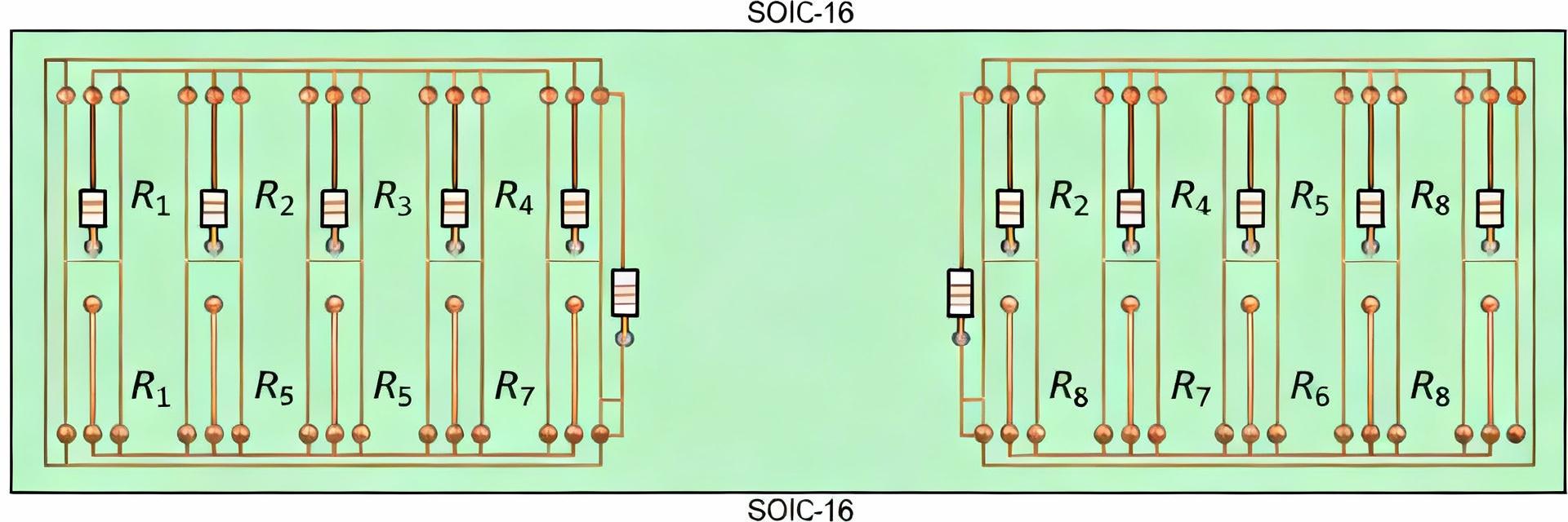
The SOMC16034K70GRZ is an isolated 8-resistor network in a 16-pin SOIC footprint optimized for compact termination and matched resistor arrays. Key numeric attributes: eight resistors, 4.7 kΩ nominal, ±2% tolerance, approximately 160 mW power per element, TCR near 100 ppm/°C, and rated for operation up to about +125 °C. Engineers consult this page to get a fast reference for specs, pinout, PCB layout guidance, and BOM/sourcing checks when fitting tight analog front ends or termination arrays into space-constrained boards.
1 — Product snapshot & where it fits (Background)
1.1 Key application zones and use cases
Point: The isolated 8-resistor SOMC16034K70GRZ is suited to matched pull-up networks, input termination, pull-down banks, sensor arrays, and compact analog front ends. Evidence: Its ±2% tolerance and ~100 ppm/°C TCR give reasonable matching and drift control for many mixed-signal tasks. Explanation: Designers pick a single SOIC resistor array over discrete parts to save board area, improve matching between channels, reduce assembly operations, and simplify inventory for repeated termination locations.
1.2 Quick spec table to lead the article
Point: Quick-reference datapoints below summarize the core specs engineers check first. Evidence: Use these entries when comparing alternatives or populating a BOM. Explanation: These bullets act as a rapid checklist before digging into full electrical limits and pin mapping.
- Nominal resistance: 4.7 kΩ
- Tolerance: ±2%
- Power per element: ~160 mW
- Number of resistors: 8, isolated network
- Package: 16‑pin SOIC (SO‑16)
- TCR: ~100 ppm/°C; operating to ~+125 °C
2 — Complete electrical specs & limits (Data analysis)
2.1 Electrical characteristics to capture
Point: Capture nominal resistance (4.7 kΩ), tolerance (±2%), TCR (~100 ppm/°C), power rating (~160 mW per element), and any maximum working voltage listed in the datasheet for safe derating. Evidence: These parameters define thermal and voltage margins and predict drift across temperature. Explanation: When designing, convert power per element to allowable voltage (Vmax ≈ sqrt(P·R)) and apply conservative derating for higher ambient temperatures or restricted thermal paths; check SOMC16034K70GRZ datasheet notes on maximum continuous voltage.
2.2 Environmental & reliability ratings
Point: Typical ratings include an extended operating temperature range and common reliability test passes. Evidence: Expect operating range to approximately −55 °C up to +125 °C and standard qualification such as thermal cycling and moisture sensitivity classification. Explanation: TCR and tolerance determine long‑term stability—lower TCR and tighter tolerance are required for precision applications, while higher TCR/tolerance is acceptable for economy terminations.
3 — Quick pinout digest & pin mapping (Data analysis / Case display)
3.1 Pin numbering and resistor-to-pin mapping
Point: The SO‑16 package has a defined pin‑1 corner; each resistor occupies two pins forming isolated elements. Evidence: Typical mapping assigns resistor ends to specific pin pairs across the 16 pins so that none are internally bussed. Explanation: For practical use, reference pin‑1 orientation on the package outline, then map pins to resistors in order (for example: pins 1–2 resistor A, pins 3–4 resistor B, etc. — consult the package drawing for exact pairs). This pinout description avoids surprises during layout and testing.
3.2 Common wiring examples
Point: Two common wiring patterns are multiple pull‑ups to a rail and ladder/voltage divider arrangements. Evidence: Use isolated elements for independent pull‑ups or connect ends to form ladder networks for ADC input scaling. Explanation: A common pitfall is assuming internal busing; this part is isolated, so choose it when independent resistors are required. Double‑check orientation to avoid reversed connections on the board.
4 — Package, footprint & PCB layout best practices (Method guide)
4.1 SO16 footprint, soldering and thermal considerations
Point: SO‑16 pad geometry and stencil strategy materially affect solder quality and thermal performance. Evidence: Stencil aperture tuning, paste ratio control, and correct pad dimensions influence fillet formation and solder volume. Explanation: Given ~160 mW per element, thermal dissipation is modest but cumulative—large copper pours or heavy traces tied to resistor pads can increase derating. Recommend standard SO‑16 pad layout, modest paste reduction under the body, and reflow profiles consistent with lead‑free solder recommendations.
4.2 Placement, routing & decoupling tips
Point: Place the resistor network close to the signals it terminates and route short traces for minimal parasitics. Evidence: Matched trace lengths matter only for differential/matched impedance cases; otherwise prioritize proximity and clean reference returns. Explanation: Use guard routing for sensitive analog lines, avoid routing high‑speed return paths underneath termination pads, and keep decoupling capacitors for adjacent active circuits as close as practical.
5 — Testing, verification & troubleshooting checklist (Method guide / Action)
5.1 Quick bench tests to validate specs
Point: A short lab checklist catches common assembly and part issues before production. Evidence: Measure room‑temperature resistance on each element, perform I–V checks at expected operating voltages, run a TCR spot check by measuring resistance across a known temperature change, and test isolation between elements. Explanation: Deviations beyond ±2% or abnormal leakage indicate assembly damage, contamination, solder bridging, or incorrect parts—address with reflow or replacement.
5.2 Common failure modes and fixes
Point: Typical failures are solder shorts, thermal overstress, incorrect footprint orientation, and ESD damage. Evidence: Visual inspection often reveals solder bridging or tombstoning; thermal damage shows discoloration. Explanation: Immediate actions include visual inspection, reflow with correct profile, cleaning flux/contaminants, and replacing suspect parts; add ESD controls to prevent recurrent damage.
6 — Sourcing, BOM integration & substitution strategy (Action suggestions / Case display)
6.1 BOM notes & procurement checklist
Point: Capture package suffixes, tape‑and‑reel vs. bulk packaging, and any lead‑form or finish variants on the BOM. Evidence: Ordering errors often stem from selecting the wrong package variant or footprint-compatible suffix. Explanation: Include resistance value, tolerance, power per element, package type (SO‑16), and thermal rating on the BOM line; verify the footprint variant and thermal spec against the chosen part number before release to manufacturing.
6.2 How to evaluate substitutes & cross-reference rules
Point: Substitution requires matching electrical and mechanical attributes closely. Evidence: Key criteria are isolated vs. bussed network type, identical nominal resistance and tolerance, equal or higher power per element, similar TCR, and identical SO‑16 footprint. Explanation: Be cautious of parts with different internal busing or pin mapping; always compare pinouts and thermal derating curves to avoid functional mismatches.
Summary
The SOMC16034K70GRZ is a compact, isolated 8-resistor SO‑16 network (4.7 kΩ nominal, ±2%, ~160 mW per element, ~100 ppm/°C) tailored for space‑constrained termination and matched resistor applications. For quick decisions focus on the specs section (electrical limits and derating), pinout mapping when laying out footprints, and the layout/test checklists before production. Action: validate pin mapping and thermal derating during PCB design, perform the bench checks listed here, and confirm BOM packaging suffixes before ordering.
- Technical Features of PMIC DC-DC Switching Regulator TPS54202DDCR
- STM32F030K6T6: A High-Performance Core Component for Embedded Systems
- APT50GH120B Datasheet Deep Dive: Specs, Ratings & Curves
- SI3402-B-GMR PoE PD Controller: Market & Specs Report
- SI3402-B-GMR Benchmarks: Real PoE Performance Insights
- EFM8BB21F16G Full Datasheet & Pinout: Specs Summary
- CP2102N-A02-GQFN20R Pinout & Footprint: Quick Data Guide
- SI53307-B-GMR Datasheet & CAD Models: Quick Specs Checklist
- SI53361-B-GMR: Latest Specs, Stock Levels & Price Guide
- SI53340-B-GM: Deep Performance Report & Key Metrics
-
 EXB-V4V120JVPanasonic Electronic ComponentsRES ARRAY 2 RES 12 OHM 0606
 -
 EXB-V4V473JVPanasonic Electronic ComponentsRES ARRAY 2 RES 47K OHM 0606
 -
 EXB-V4V823JVPanasonic Electronic ComponentsRES ARRAY 2 RES 82K OHM 0606
 -
 EXB-V4V151JVPanasonic Electronic ComponentsRES ARRAY 2 RES 150 OHM 0606
 -
 EXB-V4V181JVPanasonic Electronic ComponentsRES ARRAY 2 RES 180 OHM 0606
 -
 EXB-V4V331JVPanasonic Electronic ComponentsRES ARRAY 2 RES 330 OHM 0606
 -
 EXB-V4V152JVPanasonic Electronic ComponentsRES ARRAY 2 RES 1.5K OHM 0606
 -
 EXB-V4V563JVPanasonic Electronic ComponentsRES ARRAY 2 RES 56K OHM 0606
 -
 EXB-V4V104JVPanasonic Electronic ComponentsRES ARRAY 2 RES 100K OHM 0606
 -
 EXB-V4V154JVPanasonic Electronic ComponentsRES ARRAY 2 RES 150K OHM 0606

