-
- Contact Us
- Privacy Policy
- term and condition
- Cookies policy
MDP16031K00GD04 Datasheet: Full Spec Breakdown & Benchmarks
The MDP16031K00GD04 is a 16‑pin resistor network with a 1 kΩ nominal value, ±2% tolerance, 0.25 W per element and a 100 ppm/°C temperature coefficient — specs that make it a compact choice for matched‑resistance applications. This article provides a datasheet‑driven spec breakdown, reproducible bench benchmarks, practical design implications, and an actionable checklist for engineers.
Using measurable test procedures and PCB guidance, the goal is to help engineers validate power derating, matching behavior and board‑level thermal limits before committing to production. The write‑up focuses on repeatable methods, clear pass/fail criteria and concise procurement verifications that integrate with standard qualification workflows.
1 — Background: What MDP16031K00GD04 Is and Where It Fits
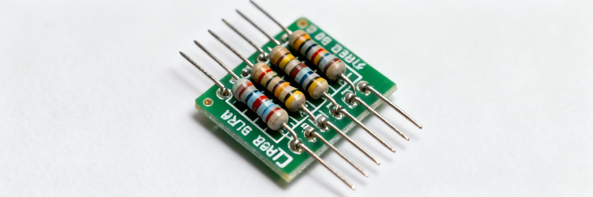
1.1 Part family overview & common use cases
Point: The device is a through‑hole resistor array (resistor network/array) intended for compact matched networks. Evidence: Typical topologies include isolated arrays and bussed configurations for pull‑ups, sensor divider arrays and trimming. Explanation: Compared with single resistors, networks save board area and improve matching by sharing thermal and process history, simplifying assembly for matched‑pair circuits.
1.2 Key mechanical summary (package & pin count)
Point: Mechanical form is a 16‑pin through‑hole package with standard DIP footprint. Evidence: Pin count and lead spacing match common DIP land patterns used for compact arrays; consult the datasheet mechanical drawing for exact dimensions. Explanation: Designers should verify hole diameter and pad annulus against their PCB house rules and plan placement to avoid interference with adjacent components.
2 — Pinout, Package Dimensions & PCB Footprint Guidance
2.1 Pinout and pin functions (how to read the datasheet table)
Point: Read the datasheet pinout table to map resistor ends and any common rails. Evidence: Standard numbering lists each element terminals and any shared pins; an annotated pinout figure clarifies which pins form each 1 kΩ element. Explanation: Create a labeled schematic symbol and board‑level silk outline to prevent swap errors during assembly and testing.
2.2 Package mechanicals, recommended footprint, thermal pads
Point: Use a conservative land pattern for through‑hole soldering and mechanical integrity. Evidence: Recommend plated‑through holes sized per PCB vendor rules, 0.8–1.0 mm drill for typical leads, and 2.54 mm pitch spacing for DIP rows. Explanation: For reliable solder fillets avoid excessive copper pours directly beneath the part; thermal vias are usually unnecessary but maintain clearance from high‑power traces.
3 — Electrical Specs & Thermal Ratings: Datasheet Deep Dive
3.1 Core electrical specs to call out
Point: Core specs determine suitability for matched networks. Evidence: Key rows are nominal resistance 1 kΩ, tolerance ±2%, power per element 0.25 W, tempco 100 ppm/°C, isolation between elements and maximum working voltage. Explanation: Tolerance and tempco directly affect divider accuracy and matched‑pair stability; include these in error budgets for ADC references and sensor dividers.
| Parameter | Value |
|---|---|
| Nominal resistance | 1 kΩ |
| Tolerance | ±2% |
| Power per element | 0.25 W |
| Tempco | 100 ppm/°C |
3.2 Thermal derating, operating temperature range & reliability notes
Point: Power handling reduces with temperature; designers must derate. Evidence: If rated 0.25 W at 25°C and linear derating to 0 W at maximum temperature, then at 70°C allowable power may be ~0.15 W. Explanation: Estimate board‑level dissipation using element I²R and account for proximity to copper pours; add a margin for long‑term drift and humidity stress in reliability budgets.
4 — Benchmarks & Test Methodology (data-driven)
4.1 Recommended test setup and measurement procedure
Point: Use controlled, repeatable measurements to validate specs. Evidence: Four‑wire resistance measurements avoid lead resistance error; use low test current to avoid self‑heating and perform thermal soak cycles to characterize tempco. Explanation: Include a temperature chamber or heat source and a data‑logger to record time‑stamped resistance vs temperature and time for reproducible trending.
4.2 Representative benchmark results to collect (and how to present them)
Point: Collect metrics that reveal real‑world behavior. Evidence: Track initial resistance spread, thermal coefficient validation, board‑level power handling and long‑term drift over accelerated hours. Explanation: Present summary tables for distribution statistics and plots for drift vs time and temperature, then interpret deviations versus datasheet specs to decide accept/reject criteria.
5 — Comparative Analysis & Application Impact
5.1 How the MDP16031K00GD04 performs versus typical resistor-network options
Point: Performance tradeoffs depend on matching and power needs. Evidence: The part offers compact matched elements with modest power per element versus discrete SMD resistors that can provide higher power or tighter tolerances. Explanation: Choose this network when space and matching outweigh higher per‑element power or when assembly simplicity is a priority.
5.2 Real-world implications: signal integrity, sensor interfaces and analog front-ends
Point: Tolerance and tempco affect front‑end accuracy. Evidence: A ±2% initial tolerance plus 100 ppm/°C drift can shift divider ratios and ADC reference levels under temperature change. Explanation: Mitigate with calibration, trimming, or placing reference networks in thermally stable regions and adding guard routing for noise‑sensitive traces.
6 — Design, Procurement & Verification Checklist
6.1 PCB and thermal layout checklist
Point: Follow concrete layout rules to protect performance. Evidence: Include correct pad sizes, keepouts for solder fillets, trace width to carry element dissipation, test points for in‑circuit verification and avoid routing high‑power traces under sensitive analog nets. Explanation: Use short thermal paths to ground pours only where necessary and maintain distance from heat sources to reduce mismatch from thermal gradients.
6.2 Datasheet validation checklist and procurement notes
Point: Validate supplied documentation before procurement. Evidence: Verify part marking, lot code traceability, and request supplier test reports or sample qualification tests. Explanation: Ask for measured lot statistics and any available burn‑in or humidity test data to ensure delivered parts meet the datasheet performance required by your application.
Key summary
- MDP16031K00GD04 provides 1 kΩ, ±2% matched elements with 0.25 W per element — suitable for compact matched networks and divider arrays.
- Thermal derating and layout matter: derate power at elevated ambient, avoid large copper under the part, and add thermal margin on sensitive paths.
- Bench tests should include four‑wire resistance, thermal soak cycles and long‑term drift plots to validate datasheet specs before production.
Frequently Asked Questions
What are the key specs I should verify on the datasheet?
Verify nominal resistance, tolerance, power per element, temperature coefficient and maximum working voltage. Also confirm mechanical drawings for hole size and pitch, and request supplier test reports for lot‑level variation to align procurement with design margins.
How should I test for thermal derating on the PCB?
Use a controlled chamber to measure resistance and power dissipation at multiple ambient temperatures. Apply the expected board current to an element, log temperature and resistance over soak intervals, and compare measured dissipation limits to the datasheet derating curve for pass/fail decisions.
When is a resistor network better than discrete resistors?
Choose a network when matching and compactness are priorities and per‑element power needs are within specified limits. Discrete resistors are preferable when higher power, tighter tolerance, or layout flexibility outweigh the benefits of integrated matching.
Conclusion (summary & key takeaways)
The MDP16031K00GD04 offers 1 kΩ elements with ±2% tolerance, 0.25 W per element and 100 ppm/°C tempco, making it a good fit for compact matched networks and divider arrays where space and matching matter. Key considerations are power derating, PCB layout and verifying matched tolerance in your application.
Use the checklist above to validate the part against your board‑level thermal and accuracy requirements before committing to production.
- Technical Features of PMIC DC-DC Switching Regulator TPS54202DDCR
- STM32F030K6T6: A High-Performance Core Component for Embedded Systems
- APT50GH120B Datasheet Deep Dive: Specs, Ratings & Curves
- SI3402-B-GMR PoE PD Controller: Market & Specs Report
- SI3402-B-GMR Benchmarks: Real PoE Performance Insights
- EFM8BB21F16G Full Datasheet & Pinout: Specs Summary
- CP2102N-A02-GQFN20R Pinout & Footprint: Quick Data Guide
- SI53307-B-GMR Datasheet & CAD Models: Quick Specs Checklist
- SI53361-B-GMR: Latest Specs, Stock Levels & Price Guide
- SI53340-B-GM: Deep Performance Report & Key Metrics
-
 EXB-V4V120JVPanasonic Electronic ComponentsRES ARRAY 2 RES 12 OHM 0606
 -
 EXB-V4V473JVPanasonic Electronic ComponentsRES ARRAY 2 RES 47K OHM 0606
 -
 EXB-V4V823JVPanasonic Electronic ComponentsRES ARRAY 2 RES 82K OHM 0606
 -
 EXB-V4V151JVPanasonic Electronic ComponentsRES ARRAY 2 RES 150 OHM 0606
 -
 EXB-V4V181JVPanasonic Electronic ComponentsRES ARRAY 2 RES 180 OHM 0606
 -
 EXB-V4V331JVPanasonic Electronic ComponentsRES ARRAY 2 RES 330 OHM 0606
 -
 EXB-V4V152JVPanasonic Electronic ComponentsRES ARRAY 2 RES 1.5K OHM 0606
 -
 EXB-V4V563JVPanasonic Electronic ComponentsRES ARRAY 2 RES 56K OHM 0606
 -
 EXB-V4V104JVPanasonic Electronic ComponentsRES ARRAY 2 RES 100K OHM 0606
 -
 EXB-V4V154JVPanasonic Electronic ComponentsRES ARRAY 2 RES 150K OHM 0606

