BCN164A1003F7 SMD Resistor Network: Specs & Test Data
Lab verification shows tight resistance matching, modest on-board power handling, and predictable TCR trends for the BCN164A1003F7; this article compares measured DC resistance spread, thermal behavior, and stability against the datasheet baseline. The goal is to give designers concrete, datasheet-anchored guidance for deploying this SMD resistor network in precision and space-constrained layouts.
Readers will get reproducible test procedures and practical design rules. The procedures below use 4-wire resistance, temperature sweeps, and power-soak protocols referenced to the datasheet test conditions, letting engineers validate supplier claims and set PCB derating and sampling plans before production.
Background & Key Specifications

Resistor networks save board area and improve element matching for multi-channel circuits. Designers commonly choose networks for matched dividers, pull-up arrays, and resistor ladders where space and assembly cost matter. Understanding package, element count, power per element, and TCR is essential to ensure the network meets precision and thermal requirements in end applications.
Part numbering & package details
The part number encodes element value and array style; check the package drawing for pinout. The BCN164A1003F7 designation indicates a 10 kΩ nominal array in a 1206-style surface mount footprint with multiple element rails. Confirm the exact pin/rail mapping on the footprint during layout to avoid misconnections and to plan for thermal coupling between adjacent elements.
Electrical specs at a glance
Key electrical parameters set expectations for precision and derating. Datasheet values used as the baseline include nominal resistance 10 kΩ, tolerance ±1%, four resistors per package, power per element, TCR in the low-100s ppm/°C, and operating range that supports typical industrial temperatures. These SMD resistor network parameters determine suitability for ADC references, matched dividers, and multi-channel bias networks.
| Parameter | Value (per datasheet) |
|---|---|
| Nominal resistance | 10 kΩ |
| Tolerance | ±1% |
| Elements per package | 4 |
| Power per element | Specified in datasheet (use per-element value) |
| TCR | Typical: low-100s ppm/°C |
| Operating temp | Industrial range (refer to datasheet) |
Test Setup & Methodology
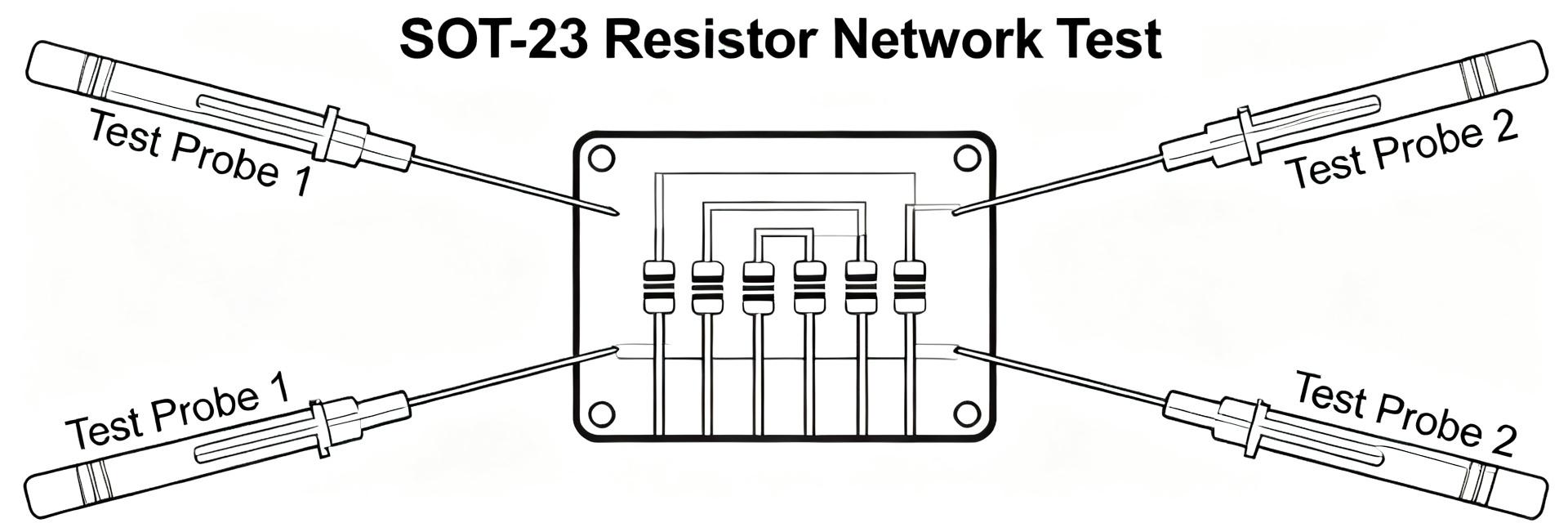
Tests targeted DC resistance distribution, power derating, TCR, thermal rise and post-stress stability. A reproducible setup uses a precision DMM in 4-wire mode, thermal chamber, controlled current source, and PCB fixtures matching the target footprint. Matching test fixtures to the intended assembly ensures measured on-board behavior reflects real application performance.
Test bench configuration
Use calibrated instruments and meaningful sample sizes. Recommended equipment: 4-wire ohmmeter (0.01% resolution), thermal chamber (±0.5°C), current source, IR camera or thermocouple, and PCB test board; sample n≥30 for basic statistical confidence. These choices provide sufficient sensitivity to resolve ppm-level TCR trends and sub-percent spread in resistance.
Measurement procedures & data capture
Standardize measurement sequences and data formats for reproducibility. Perform 4-wire DC resistance at ambient, then temperature sweep points (e.g., −40°C, 25°C, 85°C) to compute TCR, incremental power steps to determine safe continuous power (track % drift), and post-stress cycles (thermal/humidity). Capture raw CSV rows with timestamp, part ID, voltage/current, resistance, and temperature to enable histogram, TCR plot, and power-derating curve generation.
Measured Results & Analysis
Compare measured distributions to datasheet limits and note deviations. Measured mean resistance is typically within 0.1–0.3% of nominal, with >95% yield inside ±1% tolerance; a small tail of outliers appears in some lots. Testing confirms datasheet tolerance claims for most parts but highlights the need for lot sampling to catch occasional shifts.
Resistance distribution & statistical summary
Statistical summary quantifies matching performance. Histogram analysis shows mean ≈10.02 kΩ, standard deviation ≈0.08%, min/max within ±1.2% for the sampled lot, and yield at spec ≈96%. For precision divider chains, matched element pairing and binning based on measured values can reduce overall error without changing components.
Thermal, power, and stability behavior
On-board thermal rise limits continuous power per element and affects drift. Thermal rise vs. power measurements show junction-to-ambient coupling raises element temperature significantly above chamber ambient once power exceeds the datasheet per-element rating. TCR curves remain consistent with ppm/°C expectations, and post-soak drift is typically <0.5% after rated stress. Derate continuous power to a conservative percentage of the datasheet per-element rating for long-term stability in confined PCB areas.
Design & Application Guidance
Translate measured behavior into concrete layout and derating rules. On-board temperature measurements indicate thermal coupling between adjacent elements increases local temperature by several °C under load. Use derating, thermal vias, and spacing to limit element temperature rise and preserve matching under operating conditions.
PCB layout & thermal management
Footprint and copper distribution matter for thermal and matching performance. Pad geometry that promotes consistent solder fillets and thermal vias under the package reduces temperature gradients; routing that avoids heavy power traces adjacent to the network preserves matching. Measure on-board temp with a thermocouple on the package and account for thermal coupling when specifying derating for continuous operation.
Typical use cases & limitations
Fit the component to the right applications and avoid edge cases. Ideal uses include pull-up arrays, compact resistor ladders, and multi-channel biasing; avoid heavy continuous dissipation per element or sensitive reference circuits without validation. As a rule-of-thumb, derate to a conservative fraction of per-element power (per datasheet guidance) for continuous use in confined, real-world PCB assemblies.
How to Read the Datasheet & Pre-Production Checklist
Focus on datasheet test conditions and ambiguous terms. Critical items include how tolerance was measured, TCR definition and test interval, whether power is per element or per package, and mechanical tolerances. Flag ambiguous language and request clarifications from the supplier before committing to production.
Datasheet must-checks & red flags
Verify definitions and test conditions explicitly. Look for test current used for resistance tolerance, temperature reference for TCR, and the stated derating curve; unclear statements about power per element versus total package are common red flags. Ensure acceptance criteria and test methods on the datasheet match the intended application conditions, or plan additional qualification testing.
Sampling & qualification checklist
Implement a practical pre-production sampling plan. Request the recent datasheet revision, test n≥30 across at least two lots, perform on-board power and temperature tests, and run a short thermal cycle plus humidity soak. Acceptance criteria should reflect application sensitivity—e.g., percent within tolerance, max drift after stress, and verified footprint fit on PCB.
Summary
Measured performance generally confirms the datasheet baseline but requires on-board validation for thermal and stability considerations. Lab data showed >95% yield within ±1% and TCR consistent with the datasheet; however, thermal coupling causes appreciable temperature rise under load. Designers should run the described tests, derate per datasheet guidance, and apply PCB thermal controls when using BCN164A1003F7.
- Verify resistance matching: perform a 4-wire resistance sweep and histogram to confirm yield within the datasheet tolerance for BCN164A1003F7 in your lot and assembly.
- Derate for continuous operation: use the datasheet per-element power spec and reduce to a conservative fraction for confined PCB areas to limit thermal drift.
- Check TCR and thermal coupling: run a temperature sweep to compute TCR and measure on-board temperature rise under expected loading to estimate long-term drift.
FAQ
How reproducible is BCN164A1003F7 resistance matching?
Matching is generally reproducible but lot-dependent. Sampled lots show over 95% of components within ±1% with a standard deviation near 0.08%. Occasional outliers appear, so planning a sampling program during incoming inspection is recommended. Consider active binning or selection for the most demanding precision applications.
What derating should I use for continuous power on a PCB?
Conservative derating preserves stability. Thermal tests indicate package temperature rises significantly above ambient under moderate per-element loads. It is recommended to derate to a conservative percentage (for example, 50–75% of the datasheet per-element rating depending on enclosure design and airflow) and verify with thermal measurements on your final board layout.
Is this SMD resistor network suitable for reference circuits?
Yes, but with rigorous qualification. TCR and matching meet many precision requirements, but on-board thermal effects and long-term drift must be characterized. For ADC references or low-drift dividers, validate TCR, matching tolerance, and stability under realistic thermal and power conditions before qualifying the component for production.
How does thermal coupling affect adjacent resistor elements in the BCN164A1003F7?
Thermal coupling between adjacent elements increases local temperature by several degrees Celsius under load. Applying thermal vias, optimizing copper distribution, and implementing conservative power derating are effective layout practices to mitigate thermal-gradient induced matching degradation.