MPMT1003AT5 Technical Breakdown: Specs & Deep Dive
The MPMT1003AT5 appears in datasheet highlights as a compact, three‑terminal thin‑film resistor network offering tight ratio tolerance and low tracking TCR, making it suitable for precision divider and sensing tasks. Key datasheet callouts include a broad resistance range, ratio accuracy down to the few‑hundred ppm or better, and tracking as low as single‑digit ppm/°C (per datasheet). This article gives a practical, testable breakdown so you can evaluate the MPMT1003AT5 for high‑accuracy divider designs.
Purpose: You will get measured test steps, realistic implications of the Specs, PCB and soldering guidance, and a procurement checklist so you can select and validate the device in an ADC front end or sensor interface. Where numbers appear they reference the datasheet; always confirm the latest revision for ordering and qualification decisions.
Product Overview & Typical Use Cases

What the MPMT1003AT5 Is
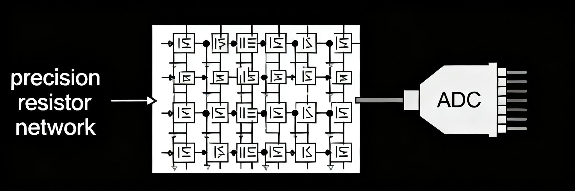
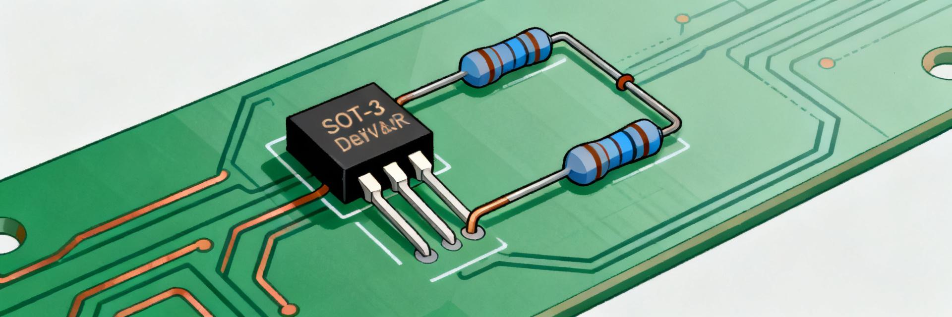
Point: The device is a three‑pin, molded SOT‑23 thin‑film resistor network arranged as two resistors in a matched divider.
Evidence: Datasheet shows two resistive elements with a common pin and two end pins in a compact package.
Explanation: You use it as a space‑efficient divider resistor in precision ADC front‑ends, sensor interfaces, reference scaling, or compact instrumentation where matched temperature behavior and ratio accuracy reduce calibration load.
Key Headline Specs to Look For
Point: Evaluate a short set of headline Specs before design.
Evidence: Typical items in the datasheet are resistance range (example: 100 Ω to 100 kΩ options), ratio tolerance (e.g., 0.01%–0.5%), tracking TCR (single‑digit ppm/°C possible), absolute TCR, power per element, package SOT‑23 and 3 pins.
Explanation: Verify available resistance options and tolerance grade for your target error budget and confirm the datasheet revision for any spec variance.
Deep-Dive: Electrical Specs & What They Mean
Resistance Range, Ratio Tolerance and Accuracy Implications
Point: Resistance values and ratio tolerance drive divider error and source loading.
Evidence: Divider output Vout = Vin · Rlow/(Rhigh+Rlow); ratio tolerance directly maps to fractional gain error.
Explanation: For example, with a nominal 1:1 divider and 0.01% ratio tolerance, worst‑case gain error is about 0.01% of Vout (use the formula ΔV/V ≈ Δratio). Choose lower resistance where source impedance and noise allow; higher resistance reduces power but increases susceptibility to input bias currents and Johnson noise.
| Option | Resistance | Typical Ratio Tolerance | Use Case |
|---|---|---|---|
| Option A | 100 Ω–1 kΩ | 0.05%–0.1% | Low impedance ADC front‑end, ultra-low noise |
| Option B | 1 kΩ–100 kΩ | 0.01%–0.5% | Higher input impedance, low power dividers |
Temperature Behavior: Tracking TCR, Absolute TCR and Stability
Point: Tracking TCR is usually more critical than absolute TCR for divider stability.
Evidence: Datasheet differentiates tracking TCR (ppm/°C between elements) and absolute TCR of each element.
Explanation: If tracking is 2 ppm/°C, a 50 °C swing yields about 100 ppm ratio drift (0.01%), which directly shifts gain. Compensate with calibration, matched temperature environment, or use on‑board temperature measurement and correction when extremely low drift is required.
Performance Testing & Evaluation Methodology
Bench Tests to Validate Specs
Point: A concise test plan validates resistance, ratio, temperature behavior, and stability.
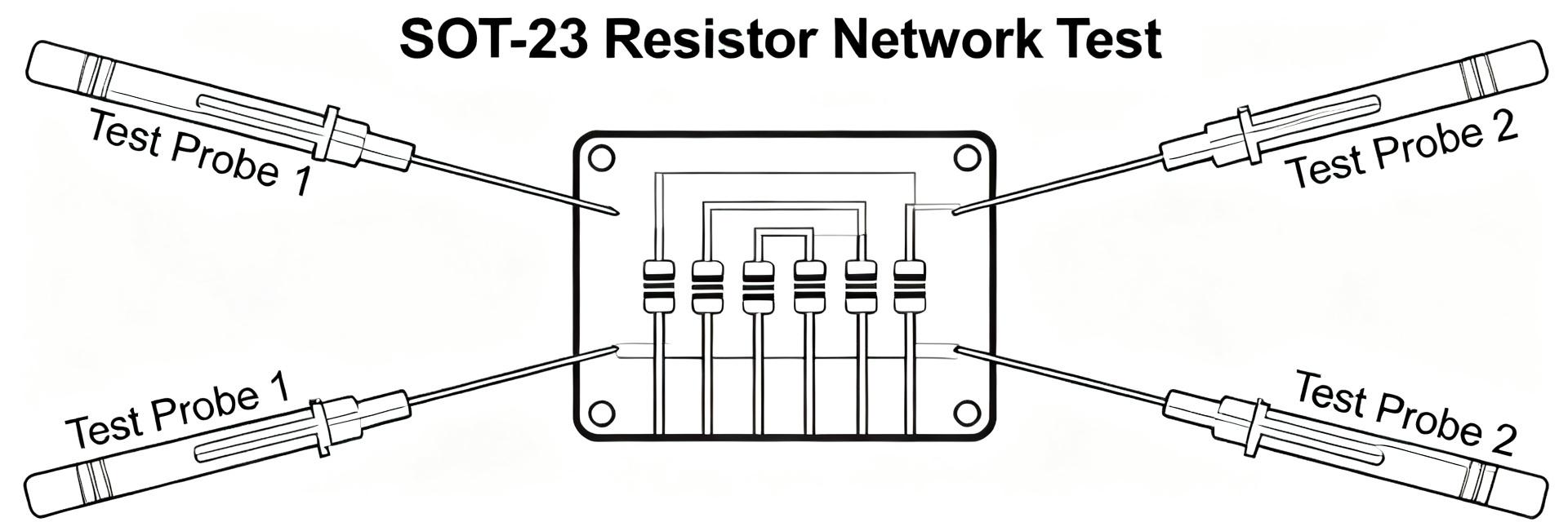
Evidence: Measure absolute resistance per element, ratio under Kelvin conditions, temperature cycling, noise, and power/thermal effects.
Explanation: Step‑by‑step: 1) measure each element with a 4‑wire DMM for tolerance, 2) apply known Vin and measure Vout to compute ratio error, 3) run temperature chamber cycles (e.g., −40 °C to +85 °C) to extract tracking TCR, 4) perform long‑term drift over weeks. Use precision instruments and record raw data for trend analysis.
Interpreting Test Results and Common Failure Modes
Point: Map measurements to datasheet limits and identify deviations.
Evidence: Common deviations include solder stress shifts, thermal gradients, or damaged parts from reflow.
Explanation: If ratio error exceeds spec but absolute resistances are near nominal, suspect differential stress or handling; if both absolutes drift, investigate material or storage issues. Use a short troubleshooting checklist: reflow profile check, board mechanical stress review, re‑measure in socketed Kelvin fixture.
PCB Integration & Design Examples
Layout, Thermal and Soldering Best Practices
Point: Layout and soldering strongly affect precision.
Evidence: Mechanical stress, thermal gradients and asymmetric copper pours create resistance shifts.
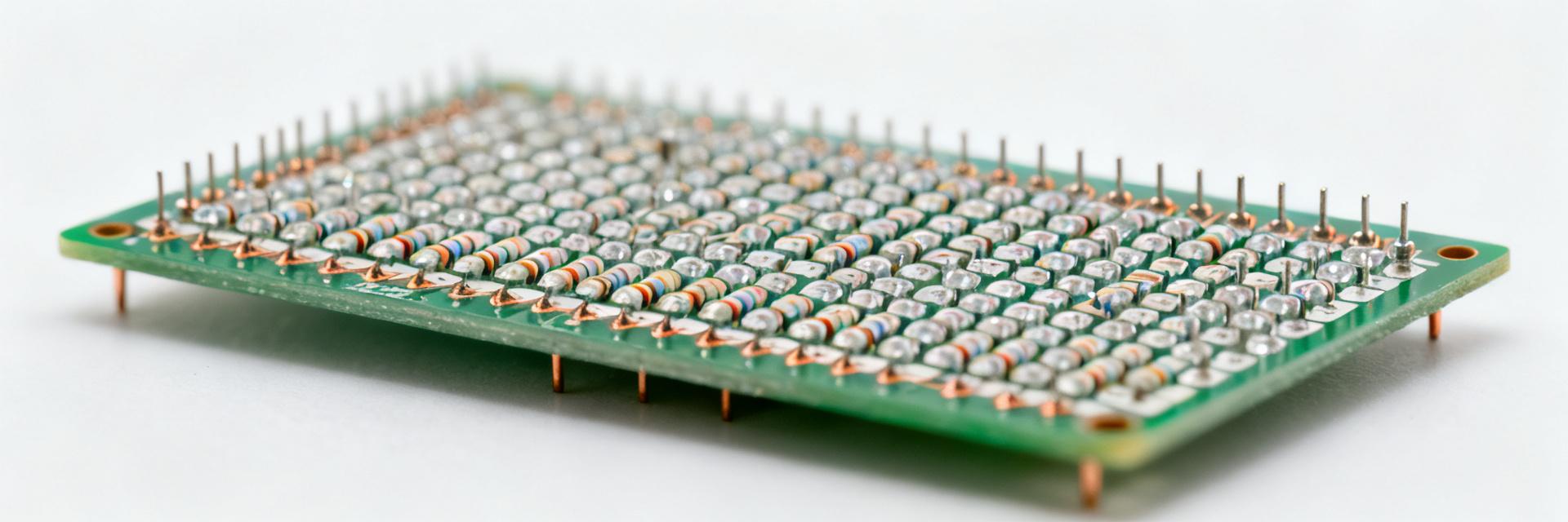
Explanation: Place the network close to the ADC input, use short Kelvin traces to the common and end pins, minimize thermals by symmetric copper and thermal reliefs, and follow a conservative reflow profile to limit package mechanical stress. Include local bypassing and avoid routing high‑current traces near the divider.
Two Compact Design Examples
Point: Practical examples show tradeoffs for low‑value and high‑voltage scaling.
Evidence: Example A — ADC front‑end uses the network as a low‑value divider to limit source impedance and noise; compute source loading and ensure ADC input bias is negligible. Example B — high‑voltage scaling places the network on the low side to balance power and impedance; select upper resistor to hold divider input impedance while keeping power within per‑element rating.
Explanation: Run the worked calculations for loading and power to confirm thermal rise stays acceptable under worst-case system rails.
Procurement, Equivalents, and Practical Checklist
Selecting the Right Variant & Spec Tradeoffs
Point: Pick value, tolerance, and TCR based on error budget and cost.
Evidence: Higher grade ratio tolerance and lower tracking TCR increase unit cost but reduce calibration load.
Explanation: Prioritize tracking when relative stability matters (dividers, ratiometric sensors); prioritize absolute TCR when single‑resistor stability vs temperature is the constraint. Account for power rating when using in high‑voltage dividers to avoid thermal mismatch.
Sourcing Checklist & Risk Mitigation
Point: A short procurement checklist lowers risk in production.
Evidence: Verify datasheet revision, part marking, packaging format, lot traceability, and storage recommendations.
Explanation: Before ordering, confirm ordering codes and packaging quantities, request sample lots for incoming inspection, and evaluate functional equivalents by comparing ratio tolerance, tracking TCR, package and pinout rather than relying on package markings alone.
Summary & Decision Guide
- The MPMT1003AT5 excels as a compact thin‑film divider with strong ratio stability; verify ratio tolerance and tracking TCR in the datasheet before selection to meet your error budget.
- Test: validate absolute resistance, ratio accuracy, and temperature tracking with Kelvin measurements and temperature cycling; follow the bench steps for reproducible validation.
- Design: use short Kelvin traces, symmetric copper, and conservative reflow to avoid stress‑induced shifts; when scaling high voltage, prioritize power rating and thermal balance.
Common Questions (FAQ)
How does ratio tolerance affect divider resistor accuracy?
Ratio tolerance directly sets the static gain error of a divider: Vout error ≈ ratio_error × Vin. If you need sub‑0.01% gain accuracy, select a network with ratio tolerance in that range (per datasheet), and validate with a precise Kelvin measurement to confirm actual assembly performance.
What is the difference between tracking TCR and absolute TCR for a resistor network?
Tracking TCR describes how two elements change relative to each other per °C and is critical for dividers since it governs ratio stability; absolute TCR is the change of each element individually. For divider resistor use, prioritize low tracking TCR to minimize gain drift over temperature swings.
Which bench equipment do you need to validate the Specs?
Use a high‑precision 4‑wire DMM or resistance bridge, a stable low‑noise source for Vout tests, a temperature chamber for controlled cycling, and Kelvin fixtures for board‑level checks. Maintain calibration traceability for instruments and define pass/fail thresholds aligned to datasheet claims before testing.
How does PCB layout mechanical stress impact MPMT1003AT5 stability?
Mechanical stress from PCB bending or asymmetric soldering causes piezo-resistive shifts in thin-film networks. Placing the SOT-23 package parallel to the board's minimum deflection axis, using symmetric copper traces, and maintaining standard thermal profiles mitigates mechanical drift.