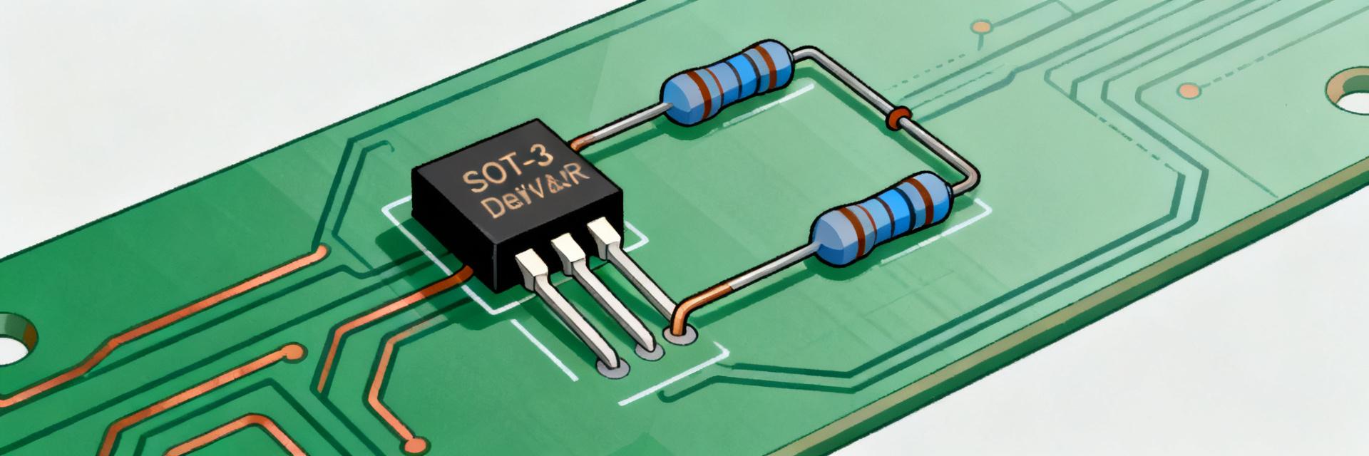
BCN164A2001F7 Full Datasheet Breakdown: Key Specs Explained
Engineers scanning a manufacturer datasheet need a concise extraction of actionable numbers: resistance values, power per element, tolerance, TCR, temperature, and package limits that drive PCB layout, thermal budget, and reliability decisions. This article pulls the decisive numeric specs from the datasheet, converts them into simple decision rules, and shows quick checks so an engineer can determine fit in minutes for BCN164A2001F7.
Point: A focused extract saves design time. Evidence: The official manufacturer datasheet typically presents a compact set of electrical and mechanical tables. Explanation: By isolating the priority specs and providing computation templates, designers avoid misreading derating curves or footprint tolerances and reduce rework risk.
1 — Background: What BCN164A2001F7 Is and Where It Fits
1.1 Part family & intended function
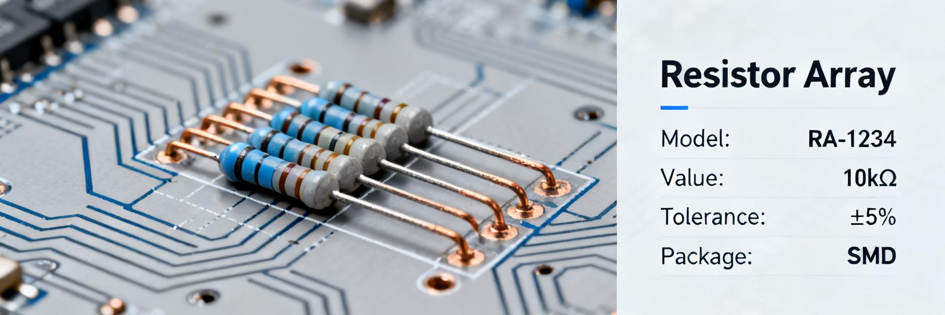
Point: BCN164A2001F7 is a resistor network/array for matched resistance applications. Evidence: Manufacturer datasheets list this class under resistor arrays with multiple elements and common configurations. Explanation: Use cases include compact voltage dividers, matched pull-ups, and resistor busses where element matching, TCR, and close tolerances matter. On a BOM, it appears as a single network reference rather than discrete resistors, described in part-number decode tables.
1.2 Package, pin count and mechanical identifiers
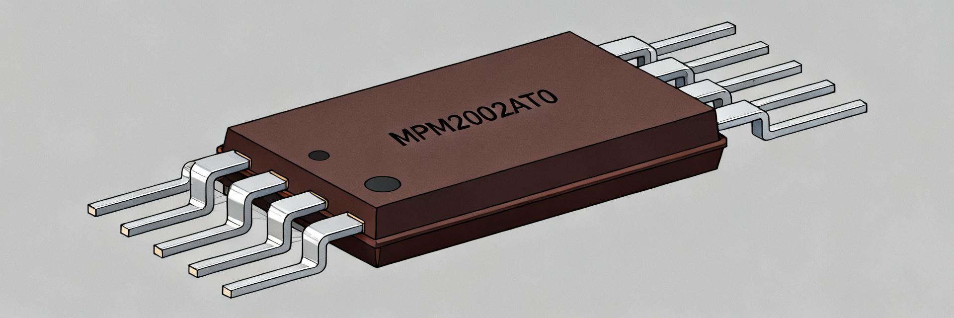
Point: Mechanical details determine footprint and assembly fit. Evidence: The datasheet includes package outline, pin count, land pattern, and pin-1 marker illustrations. Explanation: Verify land pattern, pin spacing, and thermal pad presence against PCB footprint; check package dimensions and tolerances to avoid off-grid pads, and confirm pin‑1 orientation and mechanical keep-out areas before ordering prototypes.
2 — Electrical Specs Deep Dive (Data analysis)
2.1 Static electrical specs to extract first
Point: Prioritize resistance values, tolerance, TCR, power per element, and max working voltage. Evidence: These specs appear in the electrical characteristics table of the datasheet and define circuit accuracy and limits. Explanation: For each value compute margin: required resistance ÷ spec resistance for tolerance; allowable power margin = rated power × derating factor − expected dissipation; this quick math catches mismatch pre-procurement.
2.2 Thermal & reliability limits (derating, max operating temp)
Point: Thermal derating controls safe continuous power. Evidence: Datasheets supply derating curves, thermal resistance (θJA/θJC), and soldering profiles. Explanation: Use ambient plus expected self-heating to read allowable power from the derating curve; confirm reflow profile limits and load‑life notes to estimate long‑term drift and select higher-rated arrays if needed.
3 — How to Read and Verify the Datasheet (Methods / guide)
3.1 Pinout, schematic symbol and measurement points
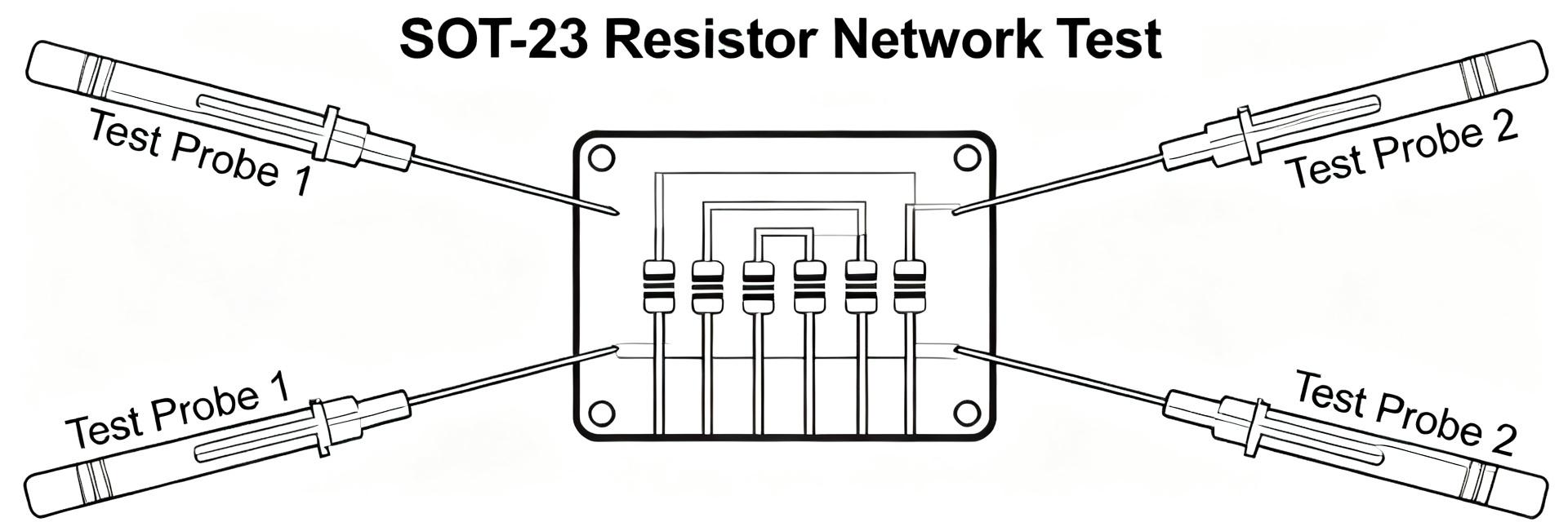
Point: Confirm internal wiring before layout or test. Evidence: Datasheet drawings show bussed vs isolated networks and wiring diagrams. Explanation: On bench, measure with a multimeter: verify each element resistance, check expected bussed nodes, and confirm insulation between isolated elements; these quick checks validate supplier parts against schematic expectations.
3.2 PCB layout, thermal management and assembly guidance
Point: Layout decisions affect thermal performance and solder reliability. Evidence: Recommended land patterns and solder mask keep-outs are found in the mechanical notes of the datasheet. Explanation: Provide copper pour or thermal pad for heat spreading, place thermal vias under large pads if allowed, and follow recommended paste stencil openings; see internal design guides such as resistor-network-layout-best-practices for templates.
4 — Application Example & Common Pitfalls (Case study)
4.1 Short application example with calculations
Point: Show a worked power/temperature margin example. Evidence: Use rated power per element and derating curve from the manufacturer datasheet. Explanation: Assume element rated 0.063 W (1/16W) at 70°C with linear derating to 0 W at 125°C. At ambient 95°C, the allowable power ratio is:
P_allowed = P_rated × [(125 - T_ambient) / (125 - 70)]
P_allowed = 0.063 × [(125 - 95) / 55] ≈ 0.034 W
This means expected continuous dissipation must not exceed 0.034 W at 95°C. Label each assumption so designers can substitute their datasheet numbers and replicate the math.
4.2 Common failure modes and troubleshooting checklist
Point: Failures usually follow spec exceedance. Evidence: Typical notes in reliability sections cite load life and thermal cycling limits. Explanation: Symptoms like drift or open circuits point to overpowering, solder cracking, or flux-related damage; inspect visually for solder fillets, measure resistances for drift, and if overloaded consider higher power rating, series resistors, or improved cooling.
5 — Selection, Substitution and Procurement Checklist (Action recommendations)
5.1 Quick spec checklist for engineers
Point: A printable checklist speeds procurement review. Evidence: Cross-reference electrical, thermal, and mechanical tables in the datasheet. Explanation: Verify resistance value(s), tolerance, TCR, power per element, package/footprint, operating temperature range, derating curve position, and pin wiring; use an internal checklist like how-to-read-datasheets before placing orders.
5.2 How to choose substitutes and what to compare
Point: Critical vs negotiable specs clarify substitution. Evidence: Datasheet comparison focuses on power, TCR, and pinout. Explanation: Match power per element, TCR, and operating temp as mandatory; package pinout and footprint must be compatible for drop-in replacements. Use the table template to compare candidates quickly.
| Spec Parameter | BCN164A2001F7 Target | Acceptable Equivalent Range |
|---|---|---|
| Resistance Value | 2.0 kΩ | Exact Match Required |
| Power per element | 0.063 W (1/16 W) | ≥ 0.063 W |
| TCR | ±200 ppm/°C | ≤ ±200 ppm/°C |
| Tolerance | ±1% | ≤ ±1% (or ±0.5% for tighter control) |
Summary
Point: The datasheet contains a few decisive numbers that determine fit. Evidence: Resistance values & tolerance, power per element, TCR, thermal/derating info, and package dimensions appear consistently in the manufacturer datasheet tables. Explanation: Use the checklist and bench measurement steps to validate suitability for BCN164A2001F7 before placing the part on a PCB; consult internal tools such as thermal-derating-calculator for quick computations.
Key Summary
- Extract resistance, tolerance, and TCR first to confirm accuracy requirements and matched-network suitability for the application.
- Read power per element and derating curves to compute continuous power margin at your ambient; confirm with thermal resistance values.
- Verify package land pattern, pin‑1 marker, and mechanical tolerances against PCB footprint to avoid assembly issues.
FAQ
How can I verify BCN164A2001F7 element values on arrival?
Measure each element with a calibrated multimeter at room temperature, confirm values within stated 1% tolerance (1980Ω to 2020Ω), and verify expected isolated nodes by checking continuity. Cross-check against the electrical table in the manufacturer datasheet and record any outliers before assembly.
What is the best way to calculate safe continuous power from the datasheet specs?
Use the rated power (0.063W at 70°C) and apply the derating curve. Determine maximum ambient operating temperature, read the allowable fraction of rated power, and compare expected dissipation to that value. Keep an extra 20% margin for manufacturing and thermal layout variance.
Which specs are non-negotiable when substituting a resistor network?
Prioritize matching power per element (0.063W), TCR (±200 ppm/°C), and physical footprint (1206 convex package with 8 pins). Circuit tolerance (1%) and resistance value (2kΩ) must meet accuracy requirements, while internal isolated wiring is mandatory to prevent shorts.
What is the internal schematic configuration of BCN164A2001F7?
The BCN164A2001F7 features an isolated resistor network layout consisting of 4 electrically independent, unbussed resistor elements across 8 pins. This allows the designer to utilize individual 2kΩ resistors with matched physical and thermal characteristics on the PCB.