BCN164A4751F7 Compact SMD Resistor Network: Key Specs
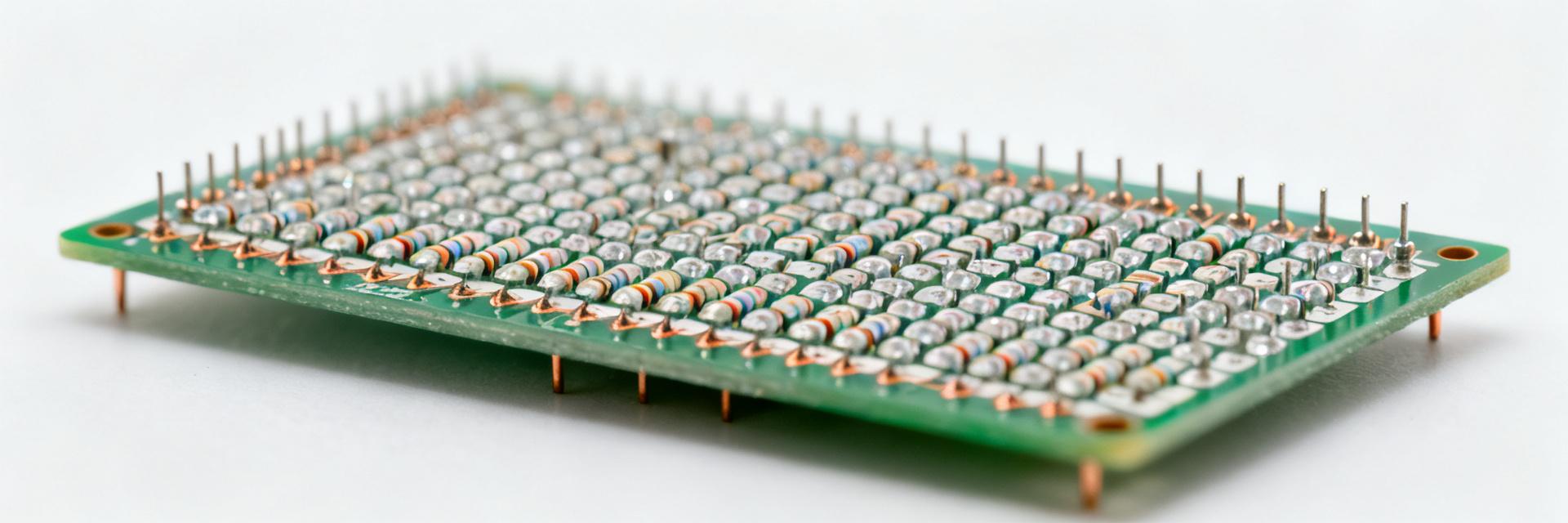
Designers routinely report 2–8× placement efficiency and lower assembly cost when replacing discrete resistors with compact arrays; the BCN164A4751F7 is positioned for space‑constrained PCBs with a balance of matching, power handling and density. Evidence from the manufacturer datasheet shows multi‑element packaging and recommended land patterns; this overview helps a hardware engineer decide if BCN164A4751F7 fits a given design.
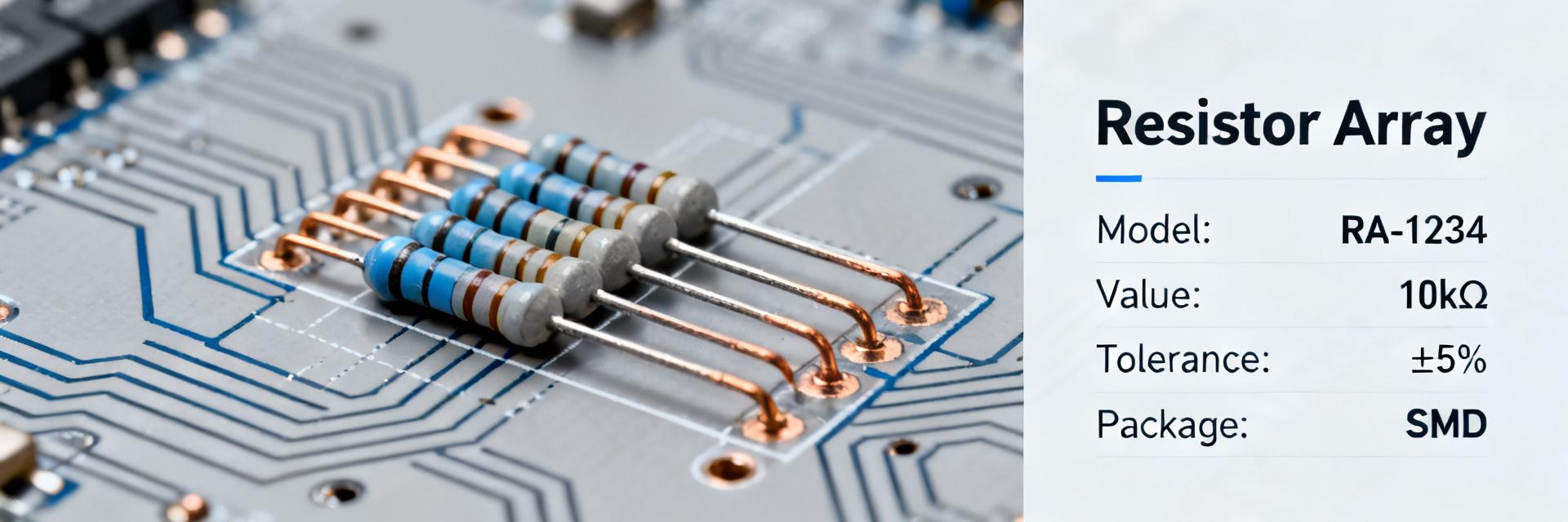
Point: BCN164A4751F7 targets high‑density designs. Evidence: manufacturer datasheet lists multi‑element topology and recommended PCB footprints. Explanation: by consolidating four resistors into one component, board area and pick‑and‑place cost fall while maintaining predictable inter‑element relationships, beneficial for pull networks, terminations and matched divider banks.
(Background) — BCN164A4751F7 at a glance
Package, pinout and physical dimensions
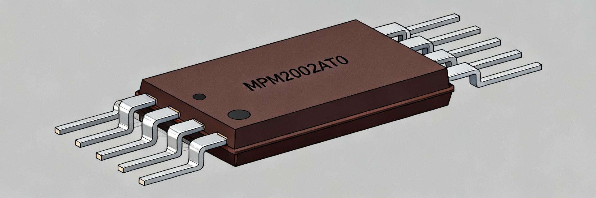
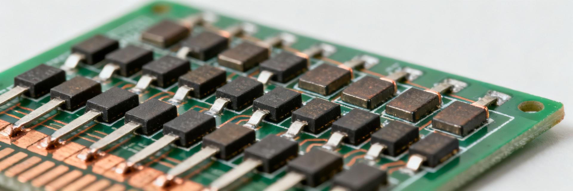
Point: package geometry determines assembly and footprint decisions. Evidence: manufacturer datasheet provides body size, pitch and pad recommendations for CAD teams. Explanation: designers should follow the recommended land pattern and orientation cues, note body thickness and pad fillet sizes, and include solder mask relief and rotation markers to avoid tombstoning and ensure reliable reflow placement.
Typical application fit and target use-cases
Point: intended uses are pull‑ups/pull‑downs, termination networks and simple divider banks. Evidence: datasheet and application notes list examples and environmental ratings. Explanation: BCN164A4751F7 suits consumer and industrial classes and can be selected for automotive class designs only after verifying specified temperature and qualification levels in the manufacturer datasheet and reliability reports.
(Data Analysis) — Electrical specifications & limits
| Electrical Metric | Specification Details | Application Relevance |
|---|---|---|
| Nominal Resistance | 4.75kΩ (Marked as 4751F) | Universal pull-up/pull-down and termination networks |
| Tolerance Rating | ±1% Standard | Guarantees reliable threshold transitions in digital/analog busses |
| Element Configuration | 4-Element Isolated Array | Supports 4 independent channels in a single 1206-equivalent package |
| Power Dissipation | Refer to Datasheet Limits | Requires thermal budgeting and land trace analysis in tight stacks |
Resistance values, tolerance and matching
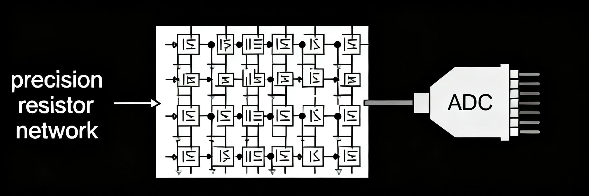
Point: available nominal resistances and matching matter for precision. Evidence: manufacturer datasheet enumerates nominal values, tolerance options and element‑to‑element matching metrics. Explanation: choose resistance and tolerance based on whether the network will be used for precision analog terminations (tight matching required) or for digital pull networks where broader tolerances are acceptable.
Power rating, TCR and derating behavior
Point: thermal limits dictate per‑element power and derating. Evidence: manufacturer datasheet specifies per‑element and package power ratings plus thermal resistance figures. Explanation: follow the published derating curve and consider local copper area, thermal vias and trace width to stay within safe junction temperatures and control drift over operating temperature as indicated by the TCR spec.
(Data Analysis) — Reliability and performance metrics
Noise, stability and long-term drift
Point: noise and drift impact precision circuits. Evidence: manufacturer datasheet lists stability and typical ppm/°C behavior and recommended test conditions. Explanation: validate long‑term drift with humidity and thermal cycling tests; for low‑noise analog use choose lower TCR and tighter stability specs and perform accelerated aging to confirm behavior aligns with datasheet figures.
ESD, surge and mechanical robustness
Point: board‑level reliability requires ESD and mechanical resilience. Evidence: manufacturer datasheet and reliability tables provide ESD thresholds, surge pulse handling and mechanical stress limits. Explanation: ensure upstream protection for sensitive buses, consider series damping where surge current is expected, and follow recommended solder and handling procedures to prevent cracking under vibration or shock.
(Design & Implementation Guide) — How to choose and integrate BCN164A4751F7
Selection checklist: electrical & mechanical fit
Point: a checklist streamlines selection. Evidence: cross‑reference system requirements with datasheet specs for resistance, tolerance, power, TCR, package and footprint. Explanation: confirm board stack‑up and copper pour, evaluate whether the array’s matching meets system impedance needs, and, if specs mismatch, consider alternative resistor values, parallel/series configurations or discrete parts as fallback options.
PCB layout, thermal and EMI best practices
Point: layout drives thermal performance and EMI. Evidence: manufacturer layout notes recommend placement, thermal vias and solder stencil patterns. Explanation: place the array near the bus or IC it serves, use short traces, add thermal relief or vias if derating requires heat spreading, and stagger ground returns to minimize coupling; follow stencil aperture guidance to avoid tombstoning and insufficient solder fillets.
(Case Examples) — Real-world application snippets
Termination and pull network example (schematic snippet guidance)
Point: arrays save space on multi‑line terminations. Evidence: typical schematics in application notes show array replacing four discretes for pull‑ups and termination. Explanation: replacing four resistors with one BCN164A4751F7 reduces impedance variability between lines, shortens layout runs, and simplifies BOM while maintaining matched resistance when the datasheet’s element‑to‑element tolerance is acceptable.
Space-constrained PCB: layout before vs after array
Point: area and assembly benefits are measurable. Evidence: board examples demonstrate component count and pick‑and‑place time reduction. Explanation: a single array footprint often uses <30% of the area of equivalent discretes and reduces BOM entries and feeder setups, delivering both area savings and lower assembly operation time on automated lines.
(Actionable checklist) — Testing, procurement and integration next steps
Qualification and testing protocol for first builds
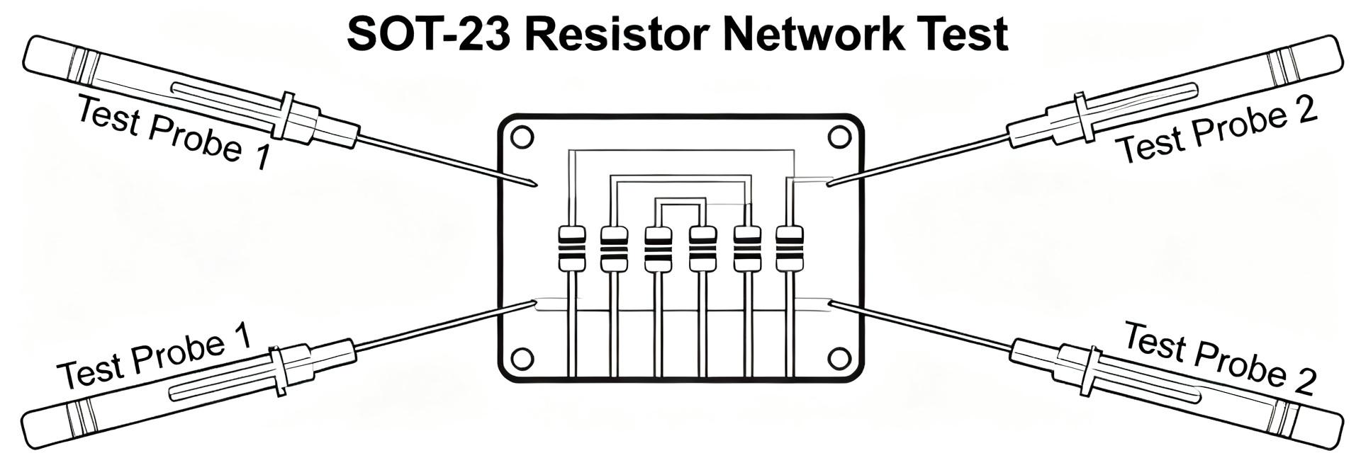
Point: a disciplined test flow reduces risk. Evidence: industry best practice and manufacturer reflow guidance recommend specific profiles and test sequences. Explanation: run visual inspection, continuity and resistance checks, thermal soak and functional tests; validate reflow within recommended temperature ranges from the datasheet and perform in‑circuit resistance and power checks on prototype boards.
Procurement, packaging and lifecycle notes
Point: procurement queries should be precise. Evidence: packaging options and lifecycle notes are listed in vendor documentation. Explanation: request tape‑and‑reel packaging for assembly, confirm MOQs and lifecycle/version status, and include the term SMD resistor array in procurement queries to ensure sourcing the correct family and request the complete manufacturer datasheet and footprint recommendations.
Summary
BCN164A4751F7 is a compact, high‑density option for designers needing a balanced combination of matching, power handling and PCB area savings; prototype integration and thermal verification against the manufacturer datasheet are recommended before volume release to ensure electrical and thermal compliance with system requirements.
Key Summary
- BCN164A4751F7 consolidates multiple resistors into one compact package, cutting placement operations and BOM complexity while preserving element relationships for matched terminations.
- Verify resistance, tolerance and element‑to‑element matching against the manufacturer datasheet when selecting for precision analog vs digital pull networks.
- Follow datasheet reflow, thermal derating and recommended land pattern; use thermal vias and copper pours if package power or TCR constraints require heat spreading.
Frequently Asked Questions
What resistance and tolerance options does BCN164A4751F7 support?
Manufacturer datasheets list the available nominal resistances and tolerance options; designers should reference the datasheet for exact values and element‑to‑element matching specifications. For precision applications, select the tightest tolerance and confirm matching metrics in the datasheet before committing to the part.
How should BCN164A4751F7 be derated for power and temperature?
Follow the derating curve and thermal resistance figures provided in the manufacturer datasheet. In practice, budget for reduced per‑element power at elevated ambient temperatures, add copper area or thermal vias as needed, and validate with thermal soak tests on a populated board to confirm junction temperatures remain within limits.
What test flow ensures BCN164A4751F7 integrates reliably on first builds?
Use a sample protocol: visual inspection after reflow, continuity and resistance checks, thermal soak under expected loading, followed by functional system tests. Cross‑check measured values with datasheet tolerances and perform accelerated humidity and thermal cycling when long‑term drift or automotive class reliability is a requirement.
What are the layout and space-saving advantages of the BCN164A4751F7 over discrete components?
A single BCN164A4751F7 array footprint typically occupies less than 30% of the active board area of four equivalent discrete resistors. It simplifies BOM management, reduces placement operations by replacing four parts with one, minimizes impedance variability between trace lines, and lowers standard pick-and-place fees on automated assembly lines.