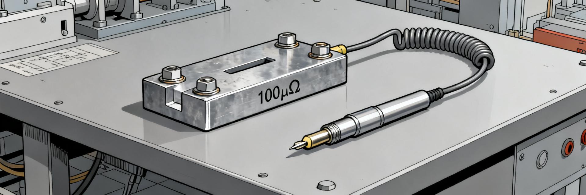
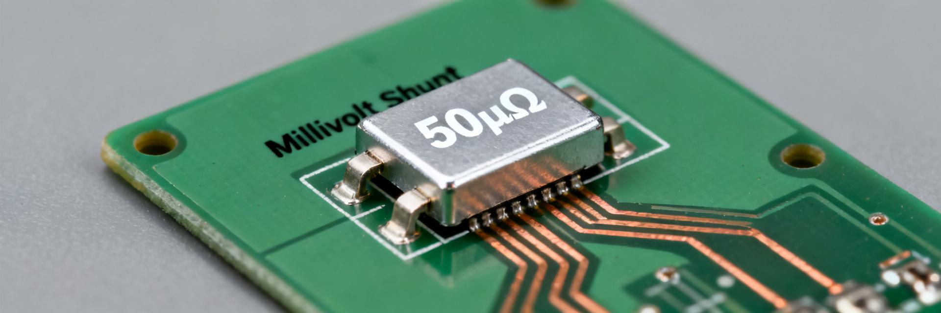
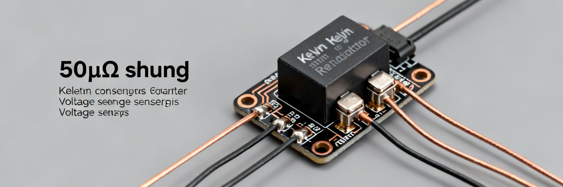
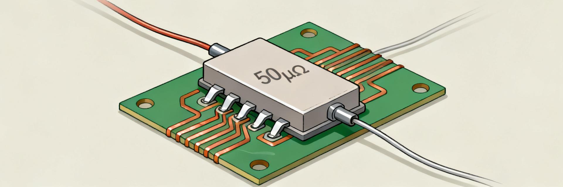
100 μΩ shunt resistor: Performance Report & Test Data
Controlled lab measurements across currents from tens to thousands of amps show millivolt-level voltage drops, measurable thermal drift, and measurable impacts on system-level accuracy — making a focused performance report essential. This introduction mentions the 100 µΩ shunt resistor once to anchor scope and clarify that the following sections prioritize measurable performance and repeatable test data for high-current sensing designs.
The article provides practical calculation methods, benchmark metrics, recommended instrumentation, representative datasets, and clear pass/fail criteria so engineers can verify parts before system integration. Emphasis is on transferability: methods and formats that produce traceable results usable in datasheet comparisons, supplier qualification, and uncertainty budgets.
1 — Background: Why use a 100 µΩ shunt resistor
Electrical role and typical applications
Point: Low-ohm current sense resistors convert high currents into small, measurable voltages. Evidence: In power electronics, battery management, EV charging, UPS and industrial drives, acceptable millivolt drops enable low-loss sensing at hundreds to thousands of amps. Explanation: A 100 µΩ current sense element yields millivolt-level V = I·R, keeping insertion loss low while matching ADC input ranges and common-mode constraints; long-tail terms include low-ohm current sense for high current applications and millivolt-level sensing for EV BMS.
Key specifications to evaluate
Point: Accuracy and stability depend on multiple specs. Evidence: Relevant parameters are resistance value/tolerance, rated current/power, TCR, thermal EMF, long-term drift, and parasitic inductance. Explanation: TCR determines ppm/°C gain shift; thermal EMF creates temperature-dependent offsets; parasitic inductance affects transients. Designers must map each spec to system error terms and include tolerance and long-term stability in the uncertainty budget.
| Spec | Effect on System | Metric |
|---|---|---|
| Resistance & Tolerance | Gain error | ppm or % |
| TCR | Temp-dependent gain shift | ppm/°C |
| Thermal EMF | Offset error vs ΔT | µV/°C |
| Parasitic inductance | Transient response impact | nH |
2 — Performance benchmarks for 100 µΩ shunt resistor
Voltage drop, power dissipation and thermal rise
Point: Calculate expected electrical and thermal loads. Evidence: Use formulas V = I·R and P = I²·R to derive mV and watts across representative currents. Explanation: For example, at 1 kA a 100 µΩ device produces V = 100 mV and P = 100 W; report ΔT vs current via measured thermal resistance (°C/W). Measurement points should include ambient, case, and sense-tip temperatures to produce ΔT vs I curves.
Linearity, noise and stability (performance metrics)
Point: Key performance metrics are linearity, noise floor, and drift. Evidence: Linearity tests compare measured V vs ideal I·R, residuals vs current reveal nonlinearity; RMS noise contributes to instantaneous uncertainty. Explanation: Report residuals in ppm of reading or %FS, present Allan deviation for low-frequency drift, and quantify short-term RMS noise in µV to support uncertainty budgets for ADC selection and filtering strategies.
3 — Test Data: 100 µΩ shunt resistor measured results
Representative datasets to collect
Point: A minimal dataset set ensures repeatable characterization. Evidence: Required runs include low-current calibration sweep, full-scale sweep, stepped transients, thermal soak and power-cycling, each repeated multiple times. Explanation: Record CSV columns: time, commanded current, measured voltage, local temperature, and ambient. Recommended repeat counts are ≥3 for each condition and sample rates matched to transient bandwidth (e.g., 1 kS/s for step tests, lower for steady sweeps).
How to present and interpret test data
Point: Clear plots and derived metrics make test data actionable. Evidence: Plot V vs I with linear fit, residuals vs I, temperature vs time under soak, and hysteresis loops for up/down sweeps. Explanation: Derive offset, gain error, TCR (ppm/°C), time-to-stable, and combined uncertainty. Present results as tables and graphs with units (mV, ppm, °C) and define pass/fail against system requirements.
4 — Test methodology & recommended instrumentation
Recommended measurement setup and wiring best practices
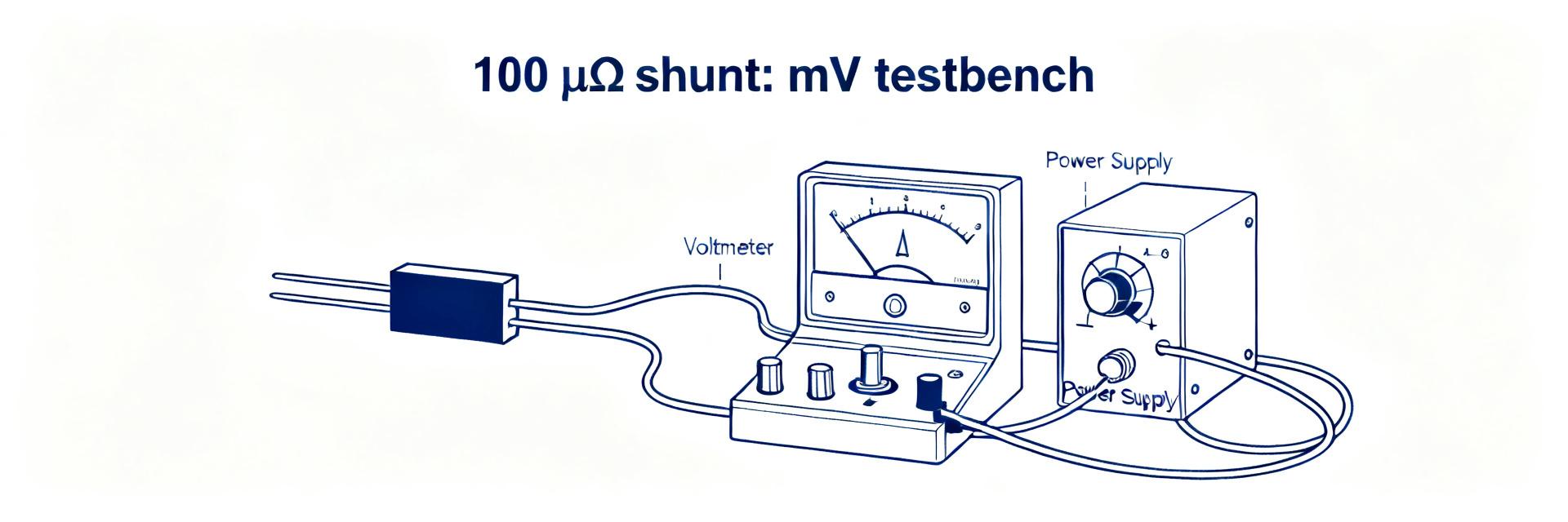
Point: Wiring and fixturing dominate low-level measurements. Evidence: Use four-terminal (Kelvin) connections, twisted and shielded sense leads, and guarded measurement nodes to minimize contact resistance and leakage. Explanation: Locate temperature sensors at the shunt body and sense terminals; use low-thermal-EMF connectors and fixtures, avoid copper heat sinks contacting sense leads, and standardize mounting orientation to control convection paths in thermal comparisons.
Instrumentation, calibration and uncertainty analysis
Point: Instrument class and calibration govern traceability. Evidence: Use precision current sources with known stability, nanovoltmeters or high-resolution ADCs, and calibrated temperature sensors. Explanation: Build an uncertainty budget listing current source error, voltmeter noise, thermal gradients, wiring contributions, and ADC quantization; combine components using root-sum-square to produce a single expanded uncertainty for reported metrics.
5 — Case studies: sample tests and anomaly investigations
High-current stress example (what to include)
Point: Document full high-current experiments for reproducibility. Evidence: Include test conditions (I profile, duration), raw summary (mean V, max ΔT, power), and observed events (drift, jumps). Explanation: Provide a result table showing steady-state V, P, ΔT and residuals; note any transient anomalies and correlate with thermal time constants to support root-cause analysis and supplier feedback.
Common failure modes and root-cause checks
Point: Typical issues are contact heating, solder degradation, and measurement lead errors. Evidence: Symptoms include sudden offset steps, rising resistance after thermal cycles, or noisy readings under vibration. Explanation: Diagnostic steps: swap shunt, re-mount with different thermal path, inspect solder joints, repeat with alternate wiring, and isolate environmental variables to confirm component vs fixturing causes.
6 — Actionable recommendations for designers and test engineers
Specification-to-system translation checklist
Point: Translate datasheet specs into system acceptance criteria. Evidence: Checklist items: specify nominal resistance, tolerance, continuous/pulse current, TCR, thermal resistance, mounting orientation and pass/fail thresholds. Explanation: Set margin for measurement chain (ADC LSB, amplifier gain, wiring errors) and require vendor samples to meet measured TCR and thermal EMF in your fixture before bulk procurement.
Best practices for integration, verification and procurement
Point: Integration and QA reduce field surprises. Evidence: Apply heatsinking or PCB copper, verify samples with the quick protocol (smoke test, DC sweep, thermal soak), and implement batch sampling. Explanation: For production, require supplier test reports, run incoming part spot checks, and include thermal-cycling and solderability tests to detect manufacturing-induced drift before assembly.
Summary
Recap: a 100 µΩ shunt resistor delivers millivolt-level sensing suitable for high-current applications, but real-world performance depends on thermal management, wiring, and measurement technique. Use the outlined benchmarks, test-data formats and uncertainty analysis to validate parts before system integration; include the 100 µΩ shunt resistor once here to anchor final recommendations.
Key summary
- Characterize V = I·R and P = I²·R across representative currents to quantify thermal rise and steady-state ΔT.
- Collect structured test data (sweeps, transients, thermal soaks) with CSV logs: time, current, voltage, temp, ambient.
- Apply four-terminal wiring, low-EMF fixtures, and an uncertainty budget combining source, meter, wiring and thermal terms.
- Specify TCR, thermal resistance and acceptance criteria in procurement; verify vendor samples under your fixture.