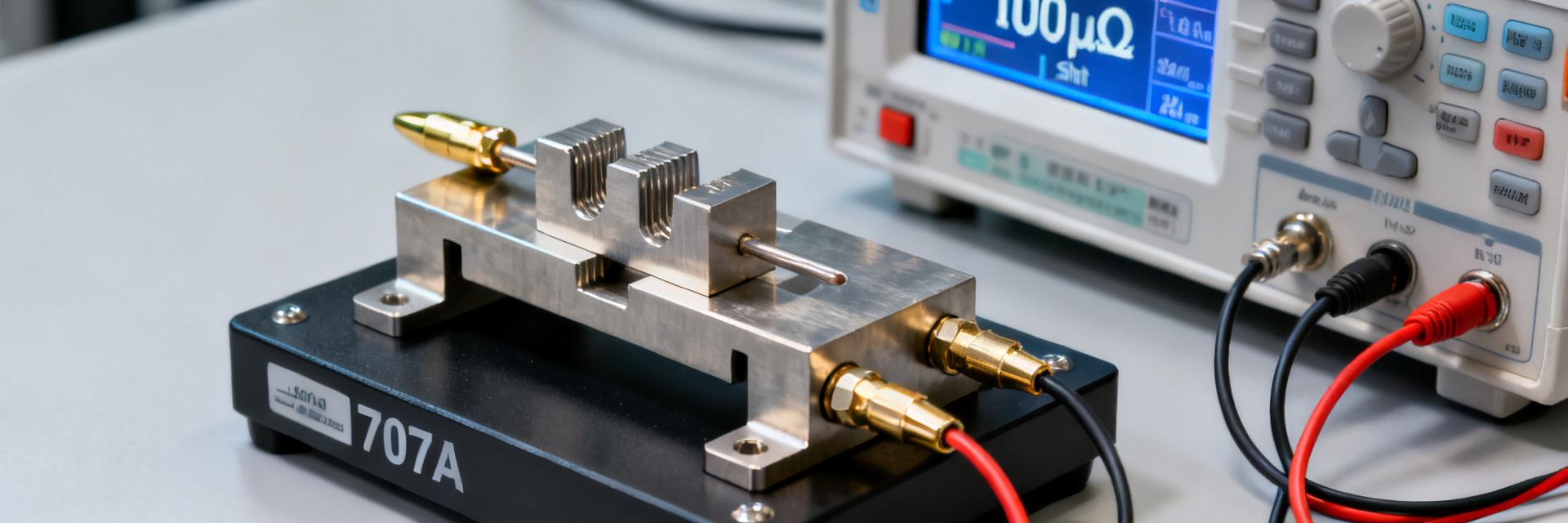
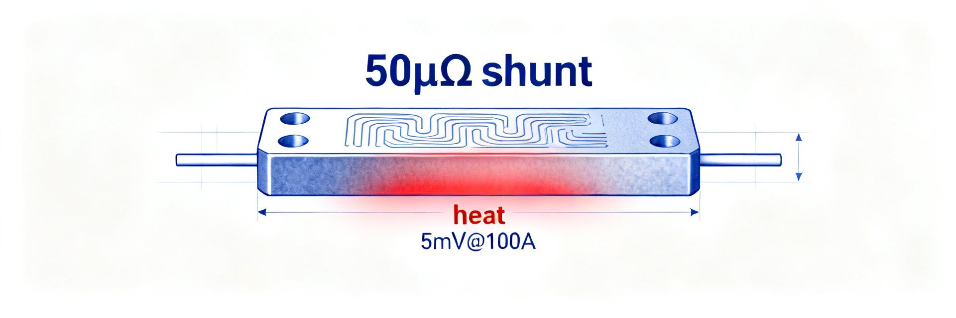
50 µΩ Shunt Resistor: Datasheet, Specs & Footprint
In modern high-current systems — battery management, EV inverters and large power supplies — measuring hundreds of amps with milliohm-level accuracy is common: a 50 μΩ shunt resistor converts 500 A into 25 mV, making it a de facto standard for precision current sensing. This article explains how to read the datasheet, verify key specs, design the PCB footprint, avoid thermal and measurement pitfalls, and run a practical integration checklist.
The goal is practical, data-driven guidance: what electrical and mechanical specs to confirm on a datasheet, how to design PCB lands and Kelvin wiring for lowest error, how to model thermal rise from power loss, and a short case example for a 600 A battery pack. The term "50 μΩ shunt resistor" appears here to anchor the discussion for design and procurement decisions.
(1/5) — Why 50 μΩ Shunt Resistors Matter
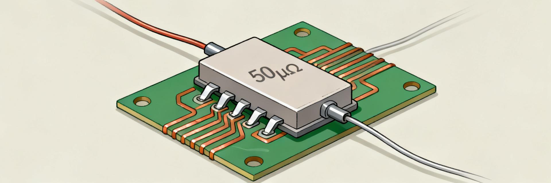
— Typical applications and design drivers
Point: Primary uses include battery packs, motor controllers, power converters and charging stations. Evidence: system-level designers choose 50 μΩ where measurable voltage and acceptable power loss intersect. Explanation: at 100 A the drop is 5 mV and at 1000 A it is 50 mV, providing a usable signal while limiting I²R losses and thermal stress for high-current sensing.
| Current (A) | Voltage (mV) | Power (W) |
|---|---|---|
| 100 | 5 | 0.5 |
| 500 | 25 | 12.5 |
| 1000 | 50 | 50 |
— Key performance trade-offs
Point: Designers balance tolerance, TCR, power rating and size. Evidence: tighter tolerance and lower TCR reduce measurement error but often raise cost and package complexity. Explanation: choose lower resistance for reduced power loss or higher for larger signal; prefer 0.5–1% tolerance and low TCR where measurement accuracy over temperature is critical.
(2/5) — Reading a 50 μΩ Shunt Resistor Datasheet — Key Specs Explained
— Electrical specifications to verify
Point: Confirm nominal resistance, tolerance, continuous and pulse current, power dissipation and TCR. Evidence: datasheets list rated continuous current, surge ratings and thermal derating curves; sense-pin arrangement and Kelvin wiring are commonly specified. Explanation: a 50 μΩ ±0.5% element at 600 A yields 30 mV nominal; TCR of 50 ppm/°C can cause measurable drift unless compensated.
| Spec | Example Value | System-Level Impact |
|---|---|---|
| Resistance | 50 μΩ ±0.5% | Directly affects accuracy |
| Rated current | 600 A cont. | Limits continuous use |
| TCR | ≤50 ppm/°C | Drift per °C |
— Mechanical and environmental specs
Point: Case size, terminal type and mounting torque determine mechanical integrity. Evidence: recommended torque, operating temperature and thermal resistance to ambient are typically provided, plus manufacturing notes for welding or plating. Explanation: verify PCB mounting guidance and specified test conditions for low-ohm measurement to ensure the quoted resistance was measured under comparable conditions.
(3/5) — Footprint, Mounting & PCB Integration for a 50 μΩ Shunt
— Recommended PCB footprint & land pattern
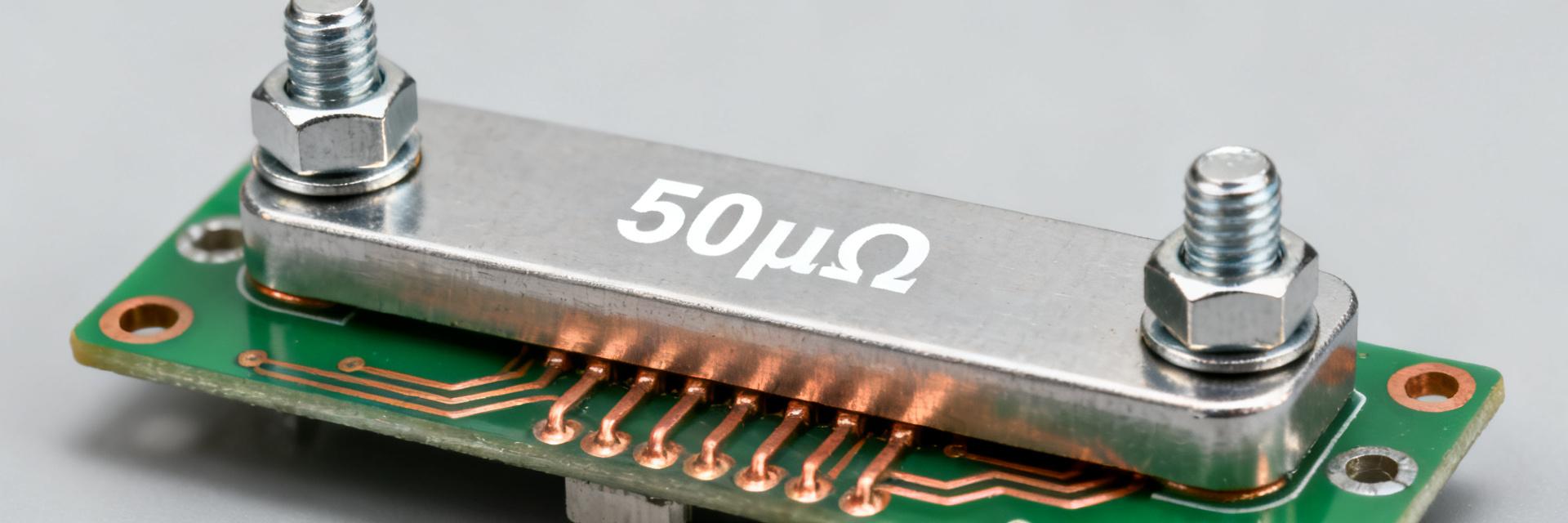
Point: Pad dimensions, hole sizes and creepage clearances must suit the shunt type. Evidence: bolt-on shunts require large plated holes and insulated clearances; surface-mount strips need broad copper lands and fillet allowance. Explanation: for bolt shunts use 6–8 mm hole diameters depending on bolt size, keep silkscreen away from high-current lands, and mark keepout areas for thin sense traces.
— Mechanical assembly and thermal routing
Point: Attachment method and copper routing control temperature rise. Evidence: bolted attachments allow replacement but add contact resistance; soldered/welded attachments give lower contact resistance but need thermal control. Explanation: use multiple thermal vias, wide copper pours and direct thermal paths to a chassis or heat spreader to limit hotspot rise and improve long-term stability.
(4/5) — Measurement Accuracy, Thermal Effects & Validation
— Kelvin connections, wiring, and measurement techniques
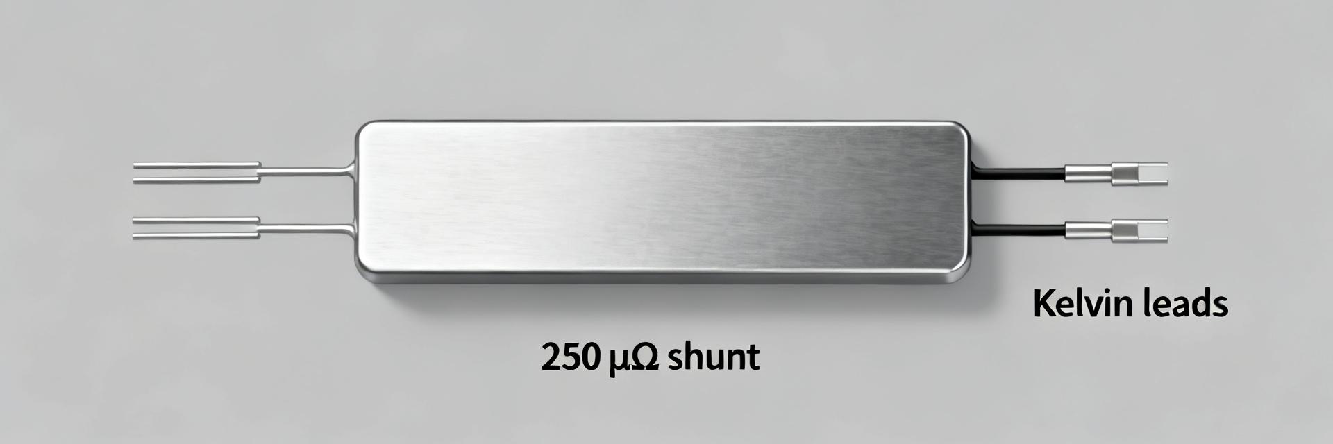
Point: True 4-wire sensing minimizes lead and contact errors. Evidence: datasheet Kelvin diagrams and recommended wiring show separate sense terminals and minimal sense trace length. Explanation: route sense traces on an inner layer or short top-layer runs, and use low-noise instrumentation amplifiers; expect tens of microvolts of common-mode noise at high currents and design filtering accordingly.
— Thermal modelling, derating and test procedures
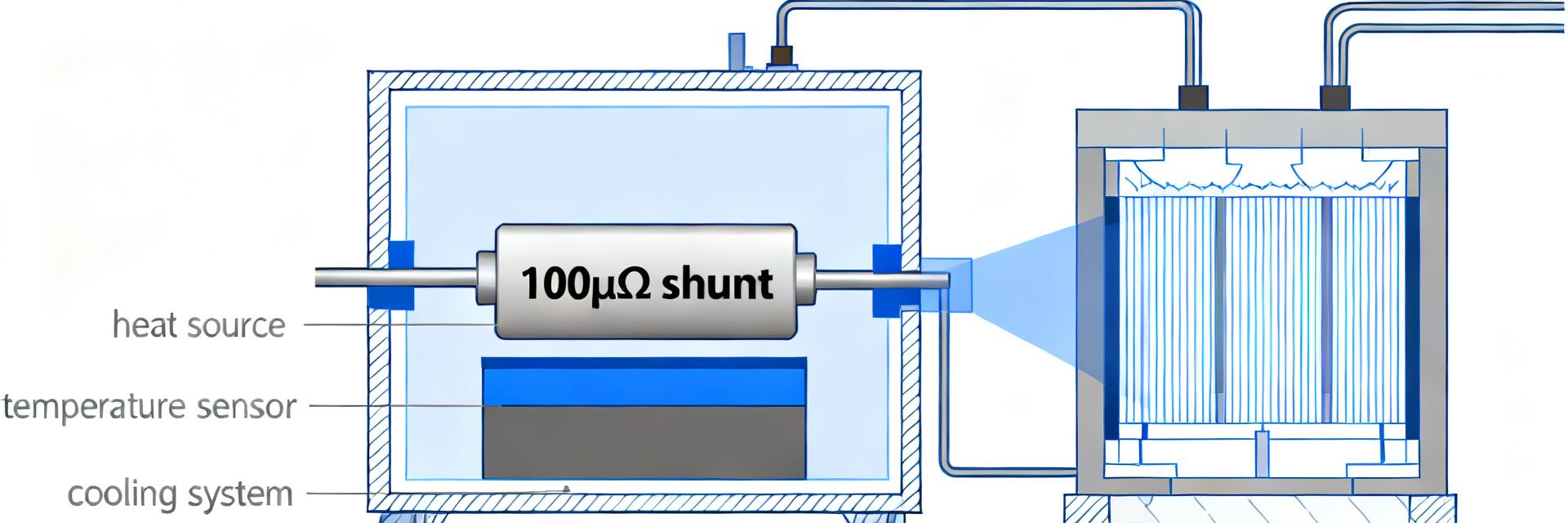
Point: Use derating curves and simple thermal math to predict rise and drift. Evidence: power = I²R yields steady-state heat; combine with thermal resistance to estimate ΔT. Explanation: validate with thermal soak and long-duration current tests, cross-check against a calibrated reference shunt, and adjust copper area or cooling if temperature or drift exceed limits.
(5/5) — Selection & Implementation Checklist + Short Case Example
— Quick selection checklist (spec-to-spec)
- Continuous Current: Ensure the continuous ampacity meets or exceeds the target application envelope.
- Target Accuracy: Determine tolerance (e.g., ±0.1% to ±1%) and matching TCR curves.
- Allowed Power Loss: Verify system cooling can handle the calculated I²R losses.
- Physical Footprint: Check bolt-on hole spacing or SMT land dimensions against manufacturing clearances.
- Traceability: Confirm test standards and calibration conditions from the device manufacturer.
— Case Example: 600 A Battery Pack Integration
Calculations:
• Signal Voltage Drop: V = I · R → 600 A × 50 μΩ = 30 mV
• Power Dissipation: P = I²R → 600² × 50e−6 = 18 W
• Thermal Drift: Temperature rise depends on system thermal resistance (R_th). If R_th is 1.5°C/W, ΔT = 1.5 × 18 = 27°C rise above ambient.
Go/No-Go Criteria: Amplifier gain must cleanly resolve a 30 mV full-scale input. If the temperature rise is within limits and the ADC SNR provides the target precision, the design passes. Otherwise, expand copper areas, add direct heatsinking, or implement active airflow cooling.
Summary
- Confirm resistance, tolerance and TCR on the datasheet to predict measurement drift for a 50 μΩ shunt resistor and choose compensation strategies for temperature-induced error.
- Design the footprint and mounting for the chosen package: bolt-on parts need large plated holes and clearances; strip shunts benefit from wide copper pours and thermal vias for heat spreading.
- Implement Kelvin wiring and low-noise amplification; validate with thermal soak, long-duration current tests, and a reference comparison to ensure in-system accuracy and stability.
FAQ
How do I choose the right 50 μΩ shunt resistor for a given current range?
Choose based on continuous and pulse current ratings, maximum allowable power loss and target measurement accuracy. Verify datasheet rated current and TCR, calculate I²R heating at peak current, and confirm the package/footprint fits your mechanical and thermal routing constraints before procurement.
What wiring and layout practices minimize error with a 50 μΩ shunt resistor?
Use true four-wire Kelvin sensing with separate low-current sense traces close to the shunt terminals, minimize sense trace length, route sense on a stable reference plane, and use wide, short high-current traces with thermal vias to lower resistance and temperature rise.
How should I validate thermal behavior and long-term accuracy for a 50 μΩ shunt resistor?
Run thermal soak and long-duration current tests at rated current, record temperature and measured resistance drift, compare to TCR expectations from the datasheet, and cross-check with a calibrated reference shunt or precision meter; adjust copper area or add cooling if drift exceeds limits.
Why is 50 μΩ considered a de facto standard in high-current systems?
At currents ranging from 500 A to 1000 A, a 50 μΩ value generates a measurable voltage drop of 25 mV to 50 mV, which provides an excellent signal-to-noise ratio for standard analog front ends while keeping power losses (12.5 W to 50 W) manageable within industrial cooling envelopes.