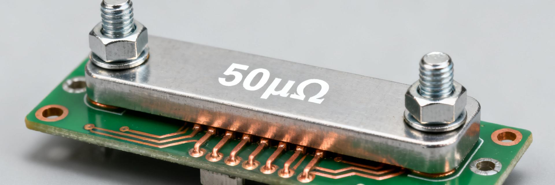
HoFL3-8518 50µΩ Shunt: Full Datasheet Analysis & Key Specs
The HoFL3-8518 50μΩ shunt produces millivolt-scale signals that require careful specification matching and measurement technique: 5 mV at 100 A and 50 mV at 1 kA. This introduction frames a data-first, practical breakdown of the HoFL3-8518, explaining datasheet interpretation, expected in-circuit behavior, and precise test and integration steps for reliable high-current sensing.
HoFL3-8518 50μΩ Shunt — Quick Overview (Background)
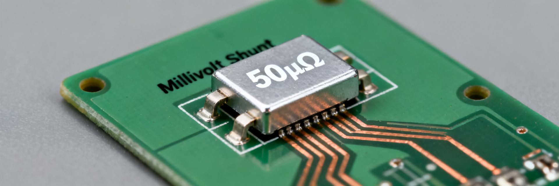
The HoFL3-8518 datasheet lists a nominal resistance of 50 μΩ with stated tolerance and mechanical dimensions that define mounting and thermal path. Understanding the package, terminal finish, and recommended torque or solder profile is essential because mechanical and thermal conditions directly affect measured resistance and long-term drift of this low-value component.
Part identifiers, package & mechanical specs
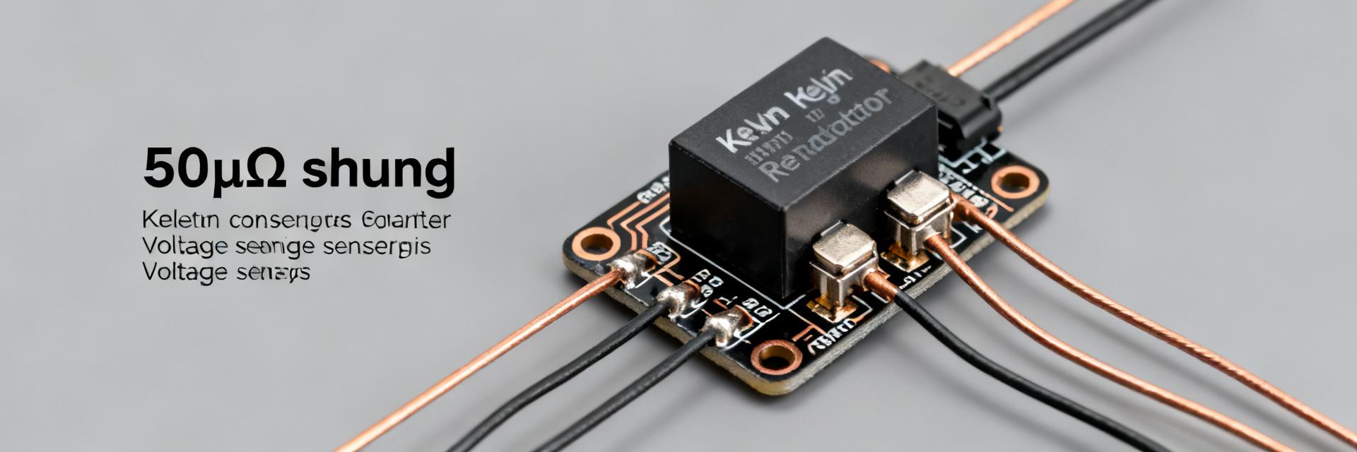
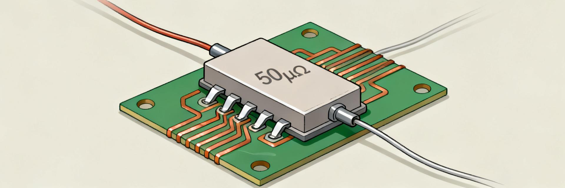
From the datasheet capture: model code, nominal resistance (50 μΩ), tolerance (±%), package outline, mounting pitch, terminal finish, and recommended torque/solder profile. Include an annotated part drawing in documentation; recommended HTML alt text: "HoFL3-8518 50μΩ shunt". Record physical tolerances and recommended torque to avoid mechanical strain that alters resistance.
Intended applications & key advantages
The part targets battery management, power distribution, DC load measurement, and charger/balancer channels where low insertion loss and high current capability are required. Advantages of a 50 μΩ shunt include minimal voltage drop and lower power loss. Quick comparisons: strip-form low-profile shunt vs. busbar — strip favors PCB integration and space; busbar offers lower thermal rise for equal current.
Electrical Specifications: Resistance, Tolerance & Power Rating (Data Analysis)
Nominal 50 μΩ — how to read tolerance & measurement methods
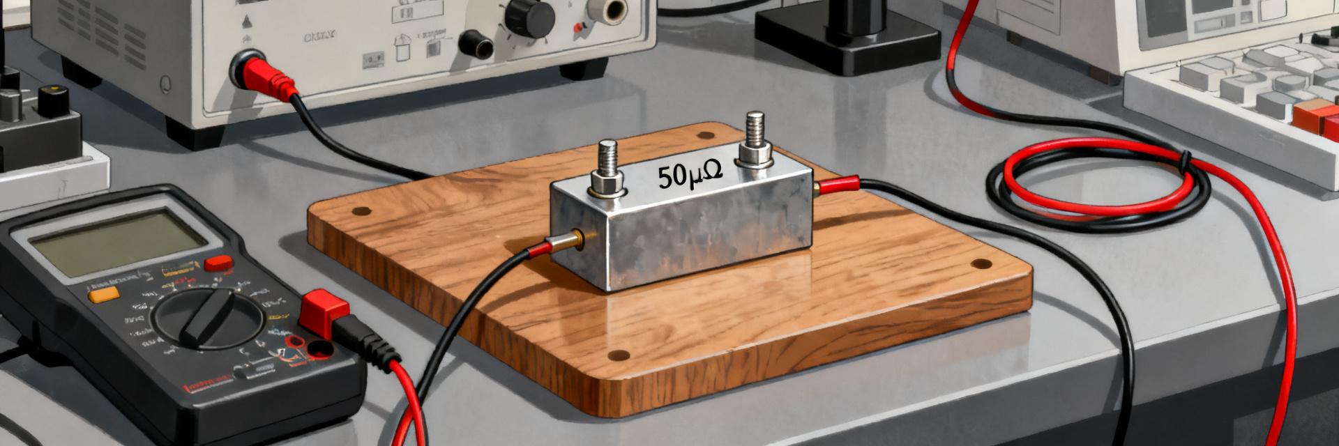
Tolerance (for example ±1%) defines the possible deviation from 50 μΩ and directly affects percent error at each current. Verify using four-wire (Kelvin) low-current ohmmeter for baseline and high-current verification using a calibrated source. V = I × R: at 50 A → 2.5 mV, 100 A → 5.0 mV, 300 A → 15.0 mV, 1 kA → 50.0 mV. Use the phrase "50 microohm shunt resistor measurement" in lab notes.
| Current (A) | Calculated Voltage Drop (mV) | Calculated Power Dissipation (W) | Thermal Challenge Class |
|---|---|---|---|
| 50 | 2.5 mV | 0.125 W | Low (Conduction via PCB) |
| 100 | 5.0 mV | 0.50 W | Low (Standard Copper Pour) |
| 300 | 15.0 mV | 4.50 W | Moderate (Vias & Active Airflow) |
| 1000 | 50.0 mV | 50.00 W | High (Heatsink / Busbar Interface) |
Power rating, derating curves & safe operating area
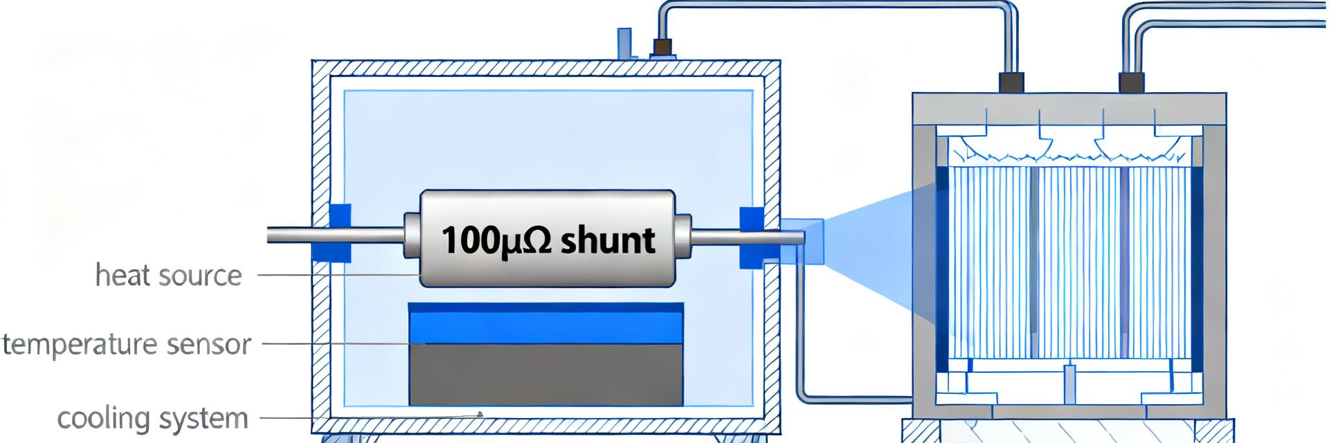
Datasheet power rating is usually steady-state with a defined thermal path; calculate dissipation P = I²R. Example: at 300 A, P = 4.5 W; at 1 kA, P = 50 W. Use derating curves that tie allowable current to ambient and PCB thermal coupling; mitigate heat with copper pours, thermal vias, or heat sinks to keep junction/board rise within specified limits.
Thermal Performance & Reliability (Data Analysis)
Temperature coefficient (TCR) and thermal stability
TCR (reported in ppm/°C) quantifies resistance change with temperature and is key to thermal stability of shunt resistor. Measure TCR by logging resistance across a controlled temperature sweep and fit ppm/°C. Compensate in-system with local temperature sensing and calibration curves or use real-time correction in firmware to maintain accuracy across operating range.
Mechanical stress, soldering, and long-term drift
Solder/reflow profiles and mechanical clamping can introduce strain that changes low-value shunt readings. Follow recommended soldering limits and torque values; perform accelerated aging (thermal cycling, humidity exposure) and monitor drift. Acceptable long-term drift should be defined in ppm over qualification cycles and tracked in a change log for serial production.
How to Integrate the HoFL3-8518 Shunt in High-Current Circuits (Method Guide)
PCB layout, Kelvin sensing & wiring best practices
Separate power and sense paths, keep Kelvin sense traces short and routed to amplifier inputs, and make current paths symmetric to minimize gradients. Recommended trace widths and copper pours should be sized for 300–1,000 A current carrying capacity as needed. Checklist: short Kelvin traces, tight sense pair routing, large thermal copper, controlled connector torque to avoid added resistance.
Amplifier selection, filtering & common-mode considerations
Select differential amplifiers with very low offset and high CMRR to handle millivolt signals plus common-mode voltages. Design trade-offs: bandwidth vs. noise — add low-pass RC filtering and differential filtering to prevent aliasing. Aim for amplifiers with offset drift in the single-microvolt range and configurable gain stages to map millivolt output into ADC full-scale without clipping.
Use Case: Battery Management & DC Load Sensing — Example Build (Case Study)
Example spec: 300 A BMS channel design using HoFL3-8518
At 300 A the shunt drops ~15 mV. For a 0–5 V ADC full scale, required gain ≈ 333 (5 V / 0.015 V). With a 12-bit ADC (1.22 mV LSB), effective current resolution ≈ 73 mA/LSB after gain. Thermal plan: allocate multi-layer copper pours, thermal vias, and forced airflow to limit board temperature rise from the ~4.5 W dissipated at 300 A.
Test plan: bench validation, thermal imaging & EMI checks
Start with four-wire low-current verification, then ramp to operational current while logging voltage and temperature. Use a thermal camera to find hotspots and record EMI behavior with switching loads. Define pass/fail: resistance drift within tolerance, acceptable temperature rise under steady load, and amplifier offset contribution below the measurement error budget.
Selection Checklist, Testing Protocols & Sourcing Considerations (Actionable)
Quick selection checklist & equivalent search terms
- Resistance: 50 μΩ; tolerance: specified %; confirm TCR and power rating.
- Package/footprint, mounting pitch, finish, recommended torque/solder profile.
- Thermal resistance, reliability data, thermal mitigation requirements.
- Search terms: "50 μΩ current sense shunt", "50 microohm high-current shunt resistor", "low-value battery shunt 50 μΩ".
Step-by-step test protocol & recommended instruments
Required instruments: four-wire µOhmmeter, programmable DC source/load, precision current source, thermal camera, data logger. Sequence: baseline room-temp DC resistance, high-current soak to operational current with stabilization, TCR sweep, mechanical torque/vibration, post-test resistance check. Recommended CSV headers: Timestamp, Current_A, Voltage_mV, Resistance_uOhm, BoardTemp_C, Notes.
Summary
The HoFL3-8518 provides millivolt-scale outputs appropriate for high-current sensing but demands careful datasheet interpretation, PCB layout, thermal design, and precision measurement. For reliable integration, apply four-wire verification, thermal mitigation, Kelvin sensing, and amplifier selection matched to the 50 μΩ shunt output to meet system accuracy targets.
- Datasheet reading: confirm nominal 50 μΩ, tolerance, and TCR to set baseline measurement error and calibration strategy for the HoFL3-8518.
- Thermal & PCB plan: calculate P = I²R (e.g., 4.5 W at 300 A) and design copper pours, vias, and airflow to limit temperature rise and drift.
- Measurement & amplifier: use four-wire baseline, Kelvin sensing, and a low-offset, high-CMRR amplifier with filtering to map millivolt signals into ADC full scale.
Additional production guidance (writer checklist)
Include visuals in documentation: annotated part drawing (alt "HoFL3-8518 50μΩ shunt"), V vs I table, derating graph, TCR vs temperature plot, PCB Kelvin wiring snippet, thermal image, and test flowchart. Use the selection checklist and test protocol during qualification and record all results in the defined CSV format for traceability.
What are the exact voltage drops of the HoFL3-8518 50μΩ shunt at typical currents?
The voltage drop scales linearly with current: at 50 A it produces 2.5 mV; at 100 A it drops 5.0 mV; at 300 A it yields 15.0 mV; and at 1 kA it outputs 50.0 mV.
How does power dissipation scale with current, and what thermal mitigation is required?
Power dissipation is calculated as P = I²R. At 300 A, the shunt dissipates 4.5 W, and at 1 kA it climbs to 50 W. Mitigation requires large multilayer copper pours, thermal vias, and potentially heat sinks or forced air cooling to prevent excessive thermal rise.
Why are four-wire Kelvin connections absolutely critical for the 50 microohm shunt?
In ultra-low resistance sensing, lead and solder contact resistances can easily exceed 50 μΩ. Four-wire Kelvin sensing isolates the current-carrying path from the measurement paths, ensuring the sense terminals only capture the millivolt-scale drop across the calibrated shunt alloy.
How is the amplifier gain calculated for a 300 A BMS system using this shunt?
At 300 A, the shunt produces 15 mV. To map this signal to a standard 0–5 V ADC input scale, the required amplifier gain is approximately 333 (5 V / 0.015 V), translating to a resolution of roughly 73 mA/LSB on a standard 12-bit ADC.