MIW50N65AT0Y-BP Datasheet: Key Electrical Characteristics & Specs
Selecting the wrong IGBT can lead to catastrophic system failures and costly downtime. For engineers designing high-power inverters or motor drives, understanding the precise Electrical Characteristics of a component like the MIW50N65AT0Y-BP is not just a preference—it’s a safety requirement. This guide breaks down the essential specs from the official Datasheet, helping you validate design margins and optimize thermal performance for 650V/50A applications in the US market.
Device Overview: Trench & Field Stop Technology
You will find that this device utilizes advanced trench gate technology combined with field stop structures. This architecture significantly reduces switching losses compared to older planar designs. The field stop layer enhances breakdown voltage capability while maintaining low conduction losses. In practical terms, this means your inverter operates cooler and more efficiently at high frequencies. The topology is specifically engineered for hard-switching environments common in industrial motor drives.
Core Architecture and Topology
The internal structure features a vertical P-N-P transistor configuration optimized for current handling. By integrating a buffer layer, the device achieves a balance between saturation voltage and turn-off speed. You should note that this hybrid approach minimizes tail current during switching events. Consequently, electromagnetic interference (EMI) noise is reduced, simplifying filter design requirements. Engineers often prefer this topology for its robustness against latch-up conditions under high di/dt stress.
Package Configuration (TO-247AB) Insights
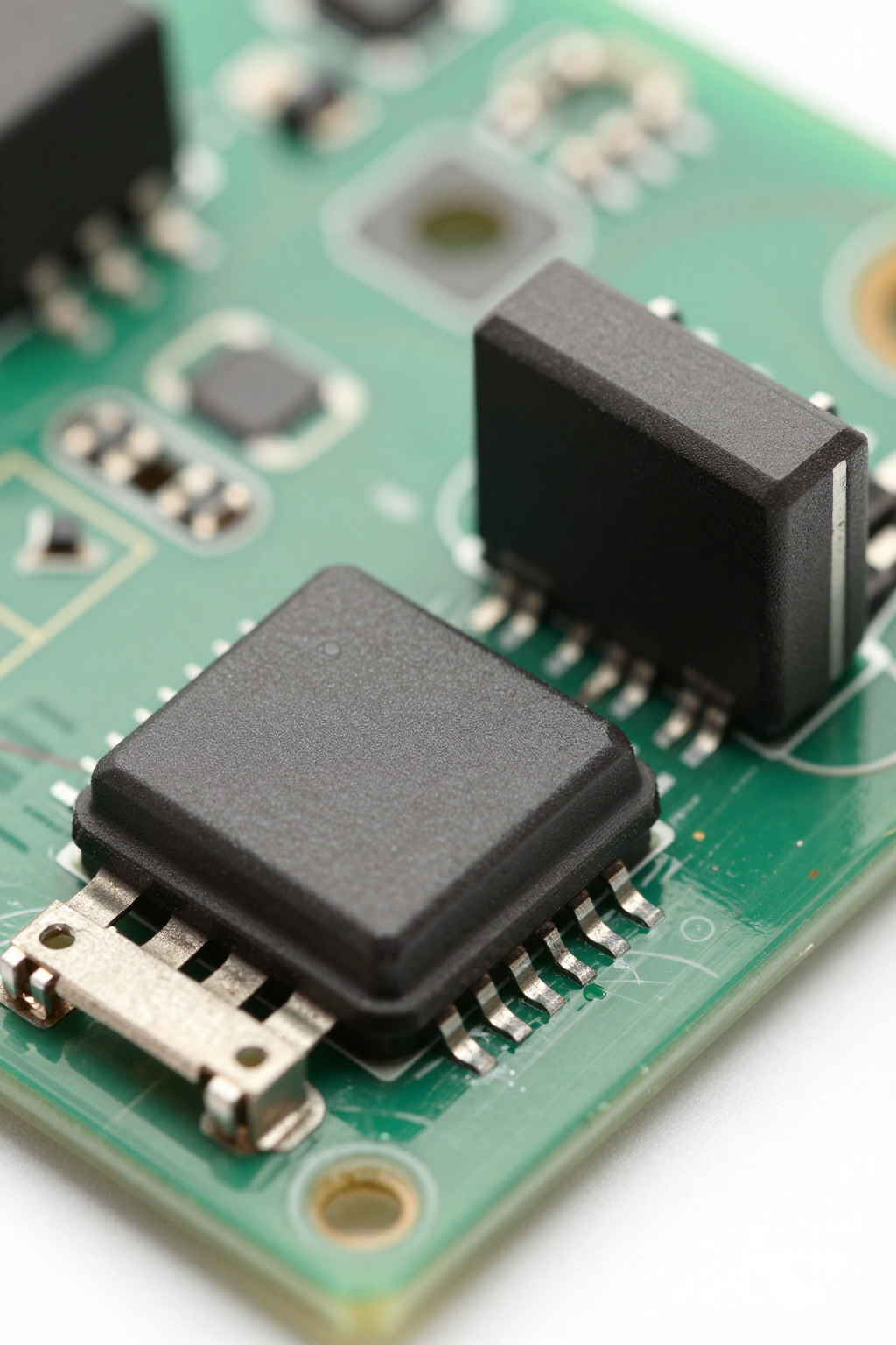
Housed in a standard TO-247AB package, the MIW50N65AT0Y-BP offers excellent mechanical stability and thermal conductivity. The wide body allows for larger die sizes, directly correlating to higher power dissipation capabilities. When mounting this component, ensure proper torque specifications to maintain consistent contact resistance with heat sinks. The isolated tab option available in some variants simplifies safety compliance in AC mains-connected systems. Always verify pinout diagrams before soldering to avoid short circuits.
Critical Static Electrical Parameters
Static parameters define the baseline performance limits of the device. You must scrutinize these values to prevent immediate failure modes during operation. The datasheet specifies absolute maximum ratings that should never be exceeded, even transiently. Understanding these limits helps you set appropriate protection thresholds in your control loop. Accurate interpretation ensures long-term reliability in demanding power electronics applications.
| Parameter | Symbol | Min | Typ | Max | Unit |
|---|---|---|---|---|---|
| Collector-Emitter Voltage | VCES | - | - | 650 | V |
| Continuous Collector Current | IC | - | - | 50 | A |
| Saturation Voltage (IC=50A) | VCE(sat) | - | 1.8 | 2.0 | V |
| Gate-Emitter Threshold Voltage | VGE(th) | 4.5 | 5.5 | 6.5 | V |
Breakdown Voltage and Leakage Current Limits
The collector-emitter breakdown voltage ($V_{CES}$) is rated at 650V, providing ample margin for typical 480V AC line rectification. At room temperature, leakage current remains negligible, typically below 1mA at rated voltage. However, as junction temperature rises, leakage increases exponentially. You should account for this thermal runaway risk when calculating standby power consumption. High leakage at elevated temperatures can distort output waveforms in precision drive systems. Therefore, thermal management becomes critical to maintaining static integrity.
On-State Voltage Drop (VCE(sat)) Analysis
At a collector current of 50A and $V_{GE}$ of 15V, the typical on-state voltage drop ($V_{CE(sat)}$) hovers around 1.8V to 2.0V. Lower saturation voltage translates directly to reduced conduction losses ($I^2R$). For your design, calculate total power loss by multiplying $V_{CE(sat)}$ by the average current over a switching cycle. A 0.2V reduction in saturation voltage can save several watts of heat generation. This efficiency gain extends the lifespan of cooling fans and heatsinks. Always check the curve graphs for temperature dependencies, as $V_{CE(sat)}$ decreases slightly with rising junction temperature.
Dynamic Switching Performance Metrics
Switching behavior dictates the operational frequency ceiling of your converter. Fast switching reduces energy lost during state transitions but may increase EMI. You need to balance speed against noise immunity. The datasheet provides detailed timing charts for resistive and inductive loads. These metrics are vital for selecting appropriate gate drivers and snubber networks.
Turn-On and Turn-Off Energy Losses
Turn-on energy ($E_{on}$) and turn-off energy ($E_{off}$) are specified at defined test conditions, usually involving specific $V_{CC}$, $I_C$, and $T_j$. For the MIW50N65AT0Y-BP, typical $E_{off}$ might range from 1.5mJ to 2.5mJ depending on gate resistance. Higher gate resistance slows switching, increasing losses but reducing voltage spikes. You should simulate these losses across your expected operating range. Total switching loss equals $(E_{on} + E_{off}) \times f_{sw}$. Minimizing this product is key to achieving high-efficiency targets in variable frequency drives.
Reverse Recovery Characteristics of the Body Diode
The integrated anti-parallel diode exhibits reverse recovery charge ($Q_{rr}$) and time ($t_{rr}$). During commutation, stored charge must be removed before blocking voltage resumes. Excessive $Q_{rr}$ causes large current spikes and additional heating. Look for soft-recovery characteristics in the datasheet curves, which indicate lower peak reverse current ($I_{RRM}$). In bridge configurations, poor diode recovery can stress the complementary switch. Selecting a device with balanced recovery traits ensures smoother commutation cycles. Verify that the diode rating matches the main IGBT current capacity to avoid asymmetrical failure risks.
Thermal Management and Reliability Data
Heat is the enemy of semiconductor longevity. Effective thermal design relies on accurate resistance data provided in the Datasheet. You must calculate the total thermal path from junction to ambient. Ignoring thermal impedance leads to premature wear-out mechanisms. Proper heatsink selection and airflow management are non-negotiable for 50A continuous operation.
Junction-to-Case Thermal Resistance (Rth(j-c))
The junction-to-case thermal resistance ($R_{th(j-c)}$) typically measures between 0.5°C/W and 0.8°C/W for this package type. This value represents the barrier to heat flow within the device itself. To keep the junction below 150°C, you must subtract case-to-sink resistance and sink-to-ambient resistance. Use the formula: $T_j = T_a + P_{total} \times R_{th(total)}$. If your calculated $T_j$ exceeds limits, improve cooling solutions immediately. Low $R_{th(j-c)}$ indicates better internal construction quality, enhancing overall system reliability.
Maximum Operating Temperature and Power Dissipation
Absolute maximum junction temperature ($T_{j,max}$) is generally 150°C or 175°C. Continuous power dissipation ($P_D$) drops linearly above a certain case temperature threshold. Consult the derating curve in the manual to determine safe operating areas. For instance, if ambient temperature exceeds 40°C, reduce current headroom accordingly. Overheating accelerates bond wire fatigue and silicon degradation. Implement temperature sensors near the module base for real-time monitoring. This proactive approach prevents thermal shutdowns and extends maintenance intervals.
Practical Design Guidelines for US Engineers
Translating specs into schematics requires careful attention to peripheral components. Gate drive strength and layout parasitics significantly influence performance. Follow industry best practices to mitigate noise and maximize efficiency. Small deviations in design can lead to disproportionate impacts on system stability.
Gate Drive Circuit Recommendations
Use a gate driver capable of sourcing/sinking sufficient peak current to charge/discharge the gate capacitance rapidly. A negative gate voltage (-5V to -15V) during off-state improves noise immunity against false triggering. Ensure short, thick traces between driver and gate pins to minimize inductance. Add a small series resistor (5Ω–20Ω) to dampen oscillations without slowing switching excessively. Isolation barriers are mandatory for safety in high-voltage applications. Test waveforms with an oscilloscope to verify clean transitions and absence of ringing.
Derating Strategies for High-Efficiency Systems
Never operate at 100% rated capacity continuously. Apply a 20–30% derating factor for extended lifespan. Consider altitude effects; reduced air density lowers convective cooling efficiency above 1,000 meters. Adjust fan speeds or heatsink size based on environmental constraints. Monitor humidity levels to prevent creepage currents across PCB surfaces. Regularly inspect thermal interface materials for drying or displacement. Systematic derating transforms theoretical specs into reliable, long-lasting field performance.
Key Takeaways
- The MIW50N65AT0Y-BP uses trench/field-stop tech for efficient 650V/50A switching.
- Low $V_{CE(sat)}$ (~1.8V) reduces conduction losses but requires strict thermal monitoring.
- Gate drive design must include negative bias and minimal trace inductance for stability.
- Apply 20–30% derating on current and temperature to ensure long-term reliability.
Frequently Asked Questions
What is the typical VCE(sat) for MIW50N65AT0Y-BP?
Under standard test conditions (50A, 15V gate), the typical saturation voltage is approximately 1.8V to 2.0V. This value decreases slightly as junction temperature rises, improving efficiency at high loads. Always refer to the specific graph in the datasheet for exact curves.
How does package type affect thermal performance?
The TO-247AB package offers lower junction-to-case thermal resistance compared to smaller SMD options. It supports higher power dissipation through better heat transfer to external sinks. Proper mounting torque and thermal paste application are critical to realizing these benefits.
Can I use this IGBT for automotive applications?
While robust, automotive-grade certification (AEC-Q101) varies by manufacturer batch. Check the specific part number suffix for automotive qualification. Standard industrial versions may lack the extreme temperature cycling tests required for vehicle environments. Verify compliance before deployment.
Why is negative gate bias recommended for this device?
Using a negative gate voltage (-5V to -15V) during the off-state significantly improves noise immunity against false triggering caused by high dv/dt transients common in hard-switching environments.