DIF075F065 IGBT Specs: Key Performance Metrics & Efficiency Data
In the demanding landscape of US industrial power electronics, selecting the right Insulated Gate Bipolar Transistor (IGBT) can make or break system efficiency. The DIF075F065 stands out as a critical component for medium-power applications, but its true value lies in the specific performance metrics that define its operational envelope. This guide dives deep into the DIF075F065 IGBT specifications, translating raw datasheet numbers into actionable insights on switching losses, thermal management, and overall efficiency data. Whether you are designing inverters, motor drives, or renewable energy converters, understanding these key parameters is essential for optimizing your circuit's reliability and cost-effectiveness.
Decoding the Core Specifications of the DIF075F065
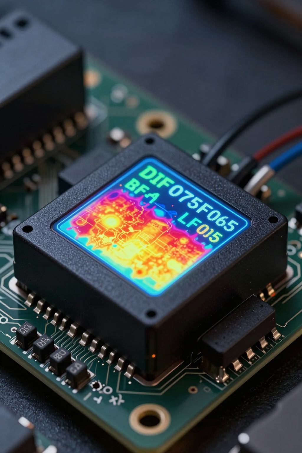
To ensure robust design margins, engineers must first interpret the fundamental electrical ratings. Misunderstanding these baseline figures often leads to premature component failure or suboptimal thermal designs.
Voltage and Current Ratings Explained
The "065" suffix typically denotes a 650V breakdown voltage class, making this device suitable for standard AC mains rectification and intermediate DC bus voltages. You should verify that your system’s peak transient voltage remains below this limit, accounting for any line spikes. The current rating defines the continuous collector current capability at a specified case temperature. For instance, operating near the maximum rated current requires strict adherence to thermal guidelines. Exceeding these limits without adequate cooling will degrade the silicon structure rapidly. Always apply a derating factor based on ambient conditions to maintain long-term reliability in high-temperature environments.
Gate Charge and Threshold Voltage Dynamics
Gate charge ($Q_g$) directly influences the speed and loss characteristics of the switching process. A lower $Q_g$ generally implies faster turn-on and turn-off times, reducing switching losses. However, it also demands a gate driver with sufficient peak current capability to charge the input capacitance quickly. The threshold voltage ($V_{GE(th)}$) determines the minimum gate-emitter voltage required to initiate conduction. In noisy industrial environments, ensuring a safe margin between the noise floor and the threshold voltage is critical to prevent false triggering. Proper selection of gate resistor values helps balance switching speed against electromagnetic interference (EMI).
Analyzing Switching Losses and Efficiency Data
Switching behavior is where theoretical specs meet practical reality. Analyzing energy loss curves allows you to predict system efficiency under various load conditions.
Turn-On and Turn-Off Energy Characteristics
Switching losses consist primarily of turn-on energy ($E_{on}$) and turn-off energy ($E_{off}$). These values are highly dependent on the collector current ($I_C$), gate resistance ($R_G$), and junction temperature ($T_j$). Typically, $E_{off}$ dominates total switching losses due to tail current effects. To minimize these losses, optimize the gate drive strength; however, be cautious not to switch too fast, which increases voltage overshoot and EMI. Plotting loss data against frequency reveals the trade-offs between high-frequency operation for smaller magnetics versus lower efficiency due to increased switching events.
Impact of Temperature on Conduction Losses
Conduction losses follow a positive temperature coefficient, meaning they increase as the junction temperature rises. At higher temperatures, the saturation voltage ($V_{CE(sat)}$) increases, leading to greater power dissipation during the on-state. This creates a feedback loop where higher losses generate more heat, further raising the temperature. Effective thermal management breaks this cycle. When calculating system efficiency data, always use the worst-case $V_{CE(sat)}$ values provided in the datasheet at elevated temperatures, rather than room temperature figures, to ensure conservative and reliable predictions.
Thermal Management and Safe Operating Area (SOA)
Heat is the enemy of power electronics. Understanding thermal impedance and SOA boundaries ensures the device survives both steady-state and transient stress.
Junction-to-Case Thermal Resistance Metrics
The junction-to-case thermal resistance ($R_{th(j-c)}$) indicates how efficiently heat moves from the silicon die to the package surface. Lower values are preferable for high-power density designs. However, this metric alone is insufficient; you must also consider the junction-to-sink resistance, which depends on the interface material quality and mounting pressure. Using high-performance thermal compounds and proper torque specifications can significantly reduce total thermal impedance. Monitor the case temperature closely, as it serves as the primary control point for most heatsink designs.
Forward-Bias and Reverse-Bias SOA Boundaries
The Safe Operating Area (SOA) defines the combinations of voltage and current where the device can operate without destruction. Forward-bias SOA covers normal conduction and switching transitions. Reverse-bias SOA is critical during freewheeling periods when the IGBT acts as a diode. Ensure your circuit design never pushes the operating point outside these boundaries, especially during short-circuit events. Many modern drivers include desaturation protection features to detect overcurrent faults and shut down the gate before the SOA limits are breached, preserving component integrity.
Practical Design Guidelines for US Engineers
Translating datasheet parameters into a physical layout requires attention to parasitic elements and signal integrity.
Optimizing Gate Drive Circuit Parameters
Design the gate drive circuit to deliver clean, sharp edges while minimizing ringing. Use isolated gate drivers if high-side switching is involved. Select gate resistors that balance switching speed with voltage overshoot control. A common mistake is using a single resistor for both turn-on and turn-off; asymmetric drive circuits allow independent tuning of $R_{g(on)}$ and $R_{g(off)}$, offering finer control over switching losses and EMI. Verify that the driver output current exceeds the peak current required by the gate charge curve at your desired switching frequency.
PCB Layout Strategies for Low Inductance
Parasitic inductance in the commutation loop causes voltage spikes that can exceed the device’s breakdown rating. Keep the loop area formed by the DC bus capacitors, the IGBT, and the shunt resistor as small as possible. Use wide copper traces for high-current paths and place decoupling capacitors extremely close to the gate-emitter terminals. Multi-layer PCBs with dedicated ground planes help reduce impedance and improve thermal dissipation. Proper layout techniques are indispensable for achieving the theoretical efficiency data promised by the component specifications.
Key Takeaways
- Verify Electrical Margins: Ensure voltage and current ratings account for transient spikes and thermal derating to prevent early failure.
- Balance Switching Speed: Optimize gate resistance to minimize $E_{on}/E_{off}$ losses while controlling EMI and voltage overshoot.
- Prioritize Thermal Paths: Minimize total thermal resistance through quality interface materials and effective heatsinking to manage conduction losses.
- Respect SOA Limits: Implement protection mechanisms to keep operation within forward and reverse bias safe areas during transients.
- Minimize Loop Inductance: Use tight PCB layouts and low-inductance connections to maximize actual system efficiency and reliability.
Frequently Asked Questions
What is the typical switching frequency for the DIF075F065?
The optimal switching frequency depends on your application’s thermal constraints and efficiency targets. While many IGBTs of this class can operate up to 20-50 kHz, practical limits are often dictated by switching losses. For high-efficiency industrial drives, frequencies around 8-16 kHz are common balances between dynamic response and thermal management. Always consult the specific datasheet graphs for loss estimation at your chosen frequency.
How does temperature affect the DIF075F065 efficiency data?
Temperature significantly impacts efficiency. As junction temperature rises, conduction losses increase due to higher $V_{CE(sat)}$. Additionally, switching losses may change depending on carrier lifetime dynamics. Designers must calculate losses at the maximum expected operating temperature, not just room temperature, to ensure the system meets regulatory efficiency standards and avoids thermal runaway in enclosed housings.
Why is gate resistance critical for this IGBT?
Gate resistance controls the charging and discharging rate of the gate capacitance. Too low a resistance causes fast switching, leading to high dv/dt, voltage overshoot, and increased EMI. Too high a resistance slows switching, increasing transition time and thus switching losses. Finding the sweet spot minimizes total power loss while maintaining signal integrity and protecting the device from destructive transients.
What are the key considerations for SOA protection?
The Safe Operating Area (SOA) defines the combinations of voltage and current where the device can operate without destruction. Forward-bias SOA covers normal conduction and switching transitions, while Reverse-bias SOA is critical during freewheeling periods. Ensure your circuit design never pushes the operating point outside these boundaries, especially during short-circuit events. Many modern drivers include desaturation protection features to detect overcurrent faults and shut down the gate before the SOA limits are breached.