MPMT20018001AT5 Datasheet Deep Dive: Specs & PCB Footprint
The MPMT20018001AT5 appears on distributor listings as a precision thin-film 2-resistor divider (2 kΩ / 8 kΩ) with ±0.1% ratio tolerance, roughly 100 mW power per element and temperature coefficients on the order of ±25 ppm/°C; this datasheet-driven summary translates those figures into practical PCB and layout guidance for designers. The goal is to convert spec review into a validated board layout with measurable reliability and repeatable test steps.
1 — Background: What the MPMT20018001AT5 Is and Where It Fits
Device family & package overview
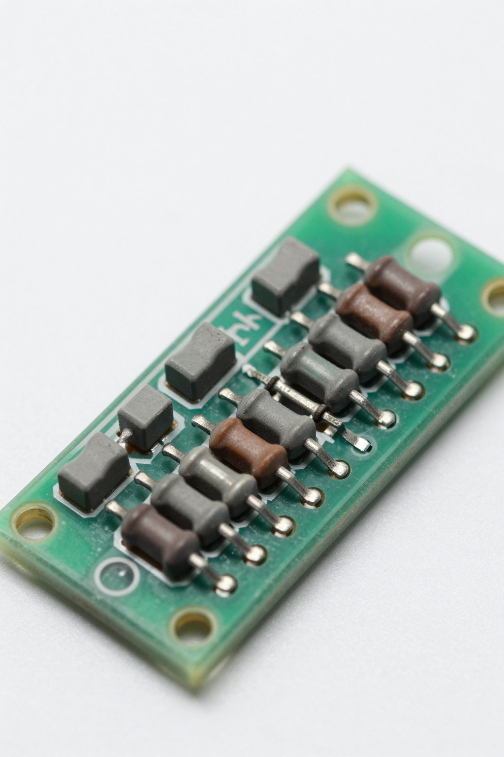
Point: The part is a molded thin-film resistor network in a SOT-23-like small outline package, commonly marked with short lot codes for traceability. Evidence: Typical devices of this family present two precision resistors internally arranged as a divider. Explanation: That geometry yields compact, matched ratio performance ideal for voltage scaling near ADC inputs or in bias networks where drift and matching dominate accuracy.
Key datasheet callouts to check first
Point: Designers should immediately read nominal resistance, tolerance/ratio, TCR (ppm/°C), power per element, maximum working voltage, absolute maximums, and the recommended land pattern. Evidence: These items determine in-circuit accuracy and reliability under thermal stress. Explanation: Interpreting ratio specs vs. absolute tolerance tells you whether system error is dominated by matching (ratio) or by single-resistor absolute error for end-to-end calibration decisions.
2 — Electrical Specs: Detailed Parameters You Need from the Datasheet
Resistance values, tolerance & ratio tracking
Point: Present the nominal pair as 2 kΩ and 8 kΩ, with a ±0.1% ratio tolerance meaning the divider ratio is tightly matched. Evidence: Ratio tracking in ppm/°C governs how the division changes with temperature, often far more important than single-element absolute tolerance for reference networks. Explanation: For ADC front ends, prioritize ratio TCR over absolute tolerance when the divider feeds a reference node used differentially.
Power, voltage limits and noise characteristics
Point: The datasheet lists ~100 mW per element continuous power; this must be derated for PCB conditions. Evidence: Thin-film networks exhibit low excess noise compared with thick-film parts, but noise still contributes to low-level measurement budgets. Explanation: Model noise only when system resolution approaches the resistor noise floor; otherwise prioritize power derating and voltage limits to prevent long-term drift.
| Parameter | Value | Unit |
|---|---|---|
| Nominal Resistance R1 | 2000 | Ω |
| Nominal Resistance R2 | 8000 | Ω |
| Ratio Tolerance | ±0.1 | % |
| Power Rating (per element) | 100 | mW |
| Temperature Coefficient | ±25 | ppm/°C |
3 — Thermal, Power-Handling & Reliability Insights
Thermal derating and PCB thermal impact
Point: Power handling depends strongly on board copper, pad size and ambient; use datasheet thermal resistance or conservative guidelines for derating. Evidence: A listed 100 mW per element is typically valid for single-sided copper and free-air; adding copper planes or larger pads increases dissipation. Explanation: Calculate steady-state temperature rise from power × thermal resistance, then apply a safety margin (30–50%) for continuous operation near hot components.
Long-term stability & reliability considerations
Point: TCR (ppm/°C) and long-term drift define calibration intervals and production qualification. Evidence: Datasheet drift figures plus manufacturer process class indicate expected ppm/year behavior. Explanation: Request or run temperature cycling, humidity and power-soak tests on sample lots to verify that tolerance stability meets your calibration window and field reliability targets.
4 — PCB Footprint & Land Pattern: From Datasheet to CAD
How to extract the recommended land pattern from the datasheet
Point: Start at the mechanical drawing and extract pad-to-pad dimensions, recommended pad lengths/widths, solder mask openings and courtyard outlines as the authoritative source. Evidence: Datasheet callouts include tolerances and suggested paste apertures; those are optimized for proper wetting and solder fillet formation. Explanation: When the datasheet gives a range, choose the middle of the range for first-pass CAD and be ready to iterate with assembly house input.
Practical footprint creation & DRC checklist (for CAD)
Point: Create a PCB footprint that balances solderability and manufacturability; include a specific PCB footprint for paste and DRC checks. Evidence: Pad fillets, paste % recommendations and stencil aperture suggestions in the datasheet reduce tombstoning and open joints. Explanation: Use rounded pad corners, define a 60–80% paste aperture for small pads, ensure silkscreen clearance and verify pick-and-place fiducials and rotation to match feeders before CAM sign-off.
5 — Layout & Placement Best Practices for Reliable Performance
Placement relative to sensitive nodes (ADC refs, op-amps)
Point: Place the divider as close as possible to the sensitive node to minimize trace-induced errors. Evidence: Short traces and minimal copper between divider and reference input reduce parasitic thermals and noise pickup. Explanation: Use solid ground pours and consider a guard trace for ultra-low leakage ADC inputs; keep noisy switching regulators and power FETs physically separated to avoid thermal gradients near the divider.
Routing, grounding and soldering considerations
Point: Route short and direct traces, avoid vias in series with divider legs, and keep a clean ground reference for low-noise circuits. Evidence: Vias add inductance and thermal discontinuities; reflow profiles affect package flatness and long-term tolerance. Explanation: Coordinate reflow profile with assembly to avoid warpage; inspect critical joints and include assembly test points for resistance checks if board space allows.
6 — Validation, Sourcing & Implementation Checklist
Test fixtures and measurement steps
Point: Implement a verification plan: DC resistance, ratio accuracy under temperature sweep, and power soak. Evidence: Measure at multiple thermal points and under rated voltage to verify datasheet figures in your PCB environment. Explanation: Use a four-wire ohm meter for absolute resistance and a precision comparator for ratio checks; document acceptance tolerances derived from datasheet min/max plus assembly variation.
Sourcing, packaging codes and procurement tips
Point: Confirm ordering codes, reel vs. cut-tape options and lot traceability before production buys. Evidence: Packaging choices affect handling and pick-and-place readiness; lot revisions can change recommended land pattern tolerances. Explanation: Order engineering samples and verify part marking and mechanical dimensions on receipt; keep a reserved sample lot for destructive or environmental testing during first builds.
Summary (actionable wrap-up)
- Confirm key specs: 2 kΩ / 8 kΩ divider geometry, ±0.1% ratio tolerance and ~100 mW per element; prioritize ratio TCR and absolute limits for accuracy and reliability in reference networks.
- Extract and implement the datasheet land pattern into CAD carefully; choose mid-range IPC-compliant pad sizes, set paste aperture to 60–80% and verify with your assembler before first run.
- Apply thermal derating on-board: calculate temperature rise from power × thermal resistance, add a conservative margin, and increase copper or pad area when continuous power approaches rated limits.
- Validate on-board performance with four-wire DC checks, temperature sweeps for ratio tracking and power-soak tests; keep samples for qualification and require lot traceability from suppliers.
FAQ
How should I verify divider accuracy on the assembled board?
Use four-wire resistance measurements for absolute values and a precision differential measurement to confirm the divider ratio. Run tests at multiple temperatures representative of operating conditions, and compare measured ratio drift to the datasheet TCR to determine if calibration or compensation is required.
What solder paste and stencil recommendations work best for small thin-film networks?
Start with 60–80% paste aperture to reduce paste slumping and tombstoning for narrow pads; use a nominal 0.1 mm stencil thickness for fine-pitch SOT-23-like parts. Coordinate with your contract assembler to adjust paste % and pod openings based on observed solder fillet formation.
Which layout mistakes most commonly degrade divider performance?
Common errors include long traces to the sensitive node, placing heat-generating components too close, and using vias in series with divider legs. These introduce thermal gradients, additional resistance and noise; correct by shortening routes, isolating heat sources and using direct pad-to-pin routing for critical legs.
Is the MPMT20018001AT5 suitable for high-frequency applications?
While primarily designed for DC and low-frequency precision scaling, its thin-film construction offers lower parasitic capacitance than thick-film alternatives. However, for RF applications above MHz levels, specific impedance matching and parasitic modeling are recommended before final selection.