IGBT Module MIF600R12C2TL-BP: Current Specs & Datasheet
The MIF600R12C2TL-BP is a 1200 V / 600 A class IGBT Module targeted at heavy industrial inverters, large motor drives, UPS systems and traction converters. This concise, datasheet-driven breakdown explains how to read the module's key ratings, how those numbers drive selection decisions, and practical integration guidance engineers can apply directly during design verification.
This article references the official datasheet tables and graphs for static ratings, switching characteristics and thermal data without linking externally. It focuses on the IGBT Module form factor, key electrical and thermal parameters, gate‑drive needs, and a short procurement checklist to accelerate evaluation and test planning.
1 — Product Background: What the MIF600R12C2TL-BP Is and Where It Fits
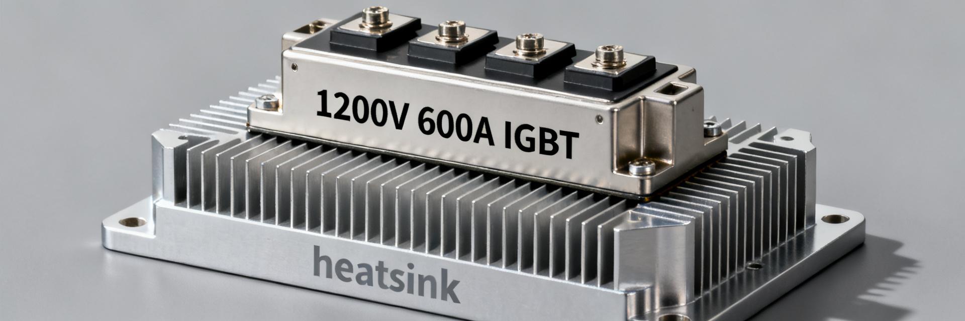
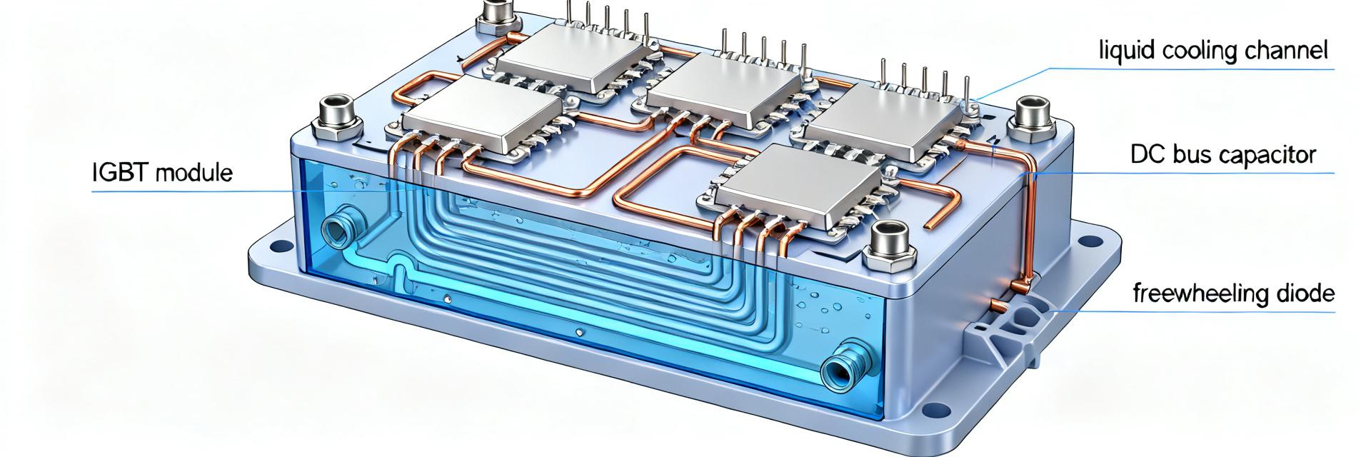
The MIF600R12C2TL-BP sits in the high-power IGBT Module category delivering nominally 1200 V blocking and 600 A current capability per datasheet class definitions. Designers choose this class for mid- to high-power applications where robustness, wide SOA margin and manageable switching loss are priorities, such as medium-voltage inverter stacks, traction inverters and large industrial motor drives requiring conservative derating and good thermal management.
1.1 Module class & intended applications
This 1200V/600A class IGBT module is suitable where continuous currents approach several hundred amperes and bus voltages require 1.2 kV blocking. Typical use cases include multi-kW motor drives, photovoltaic string inverters and locomotive traction stages. Use long-tail search terms like "1200V 600A IGBT module applications" or "MIF600R12C2TL-BP use cases" when researching alternate parts or application notes to compare SOA, switching loss and package features.
1.2 Mechanical package & pinout overview
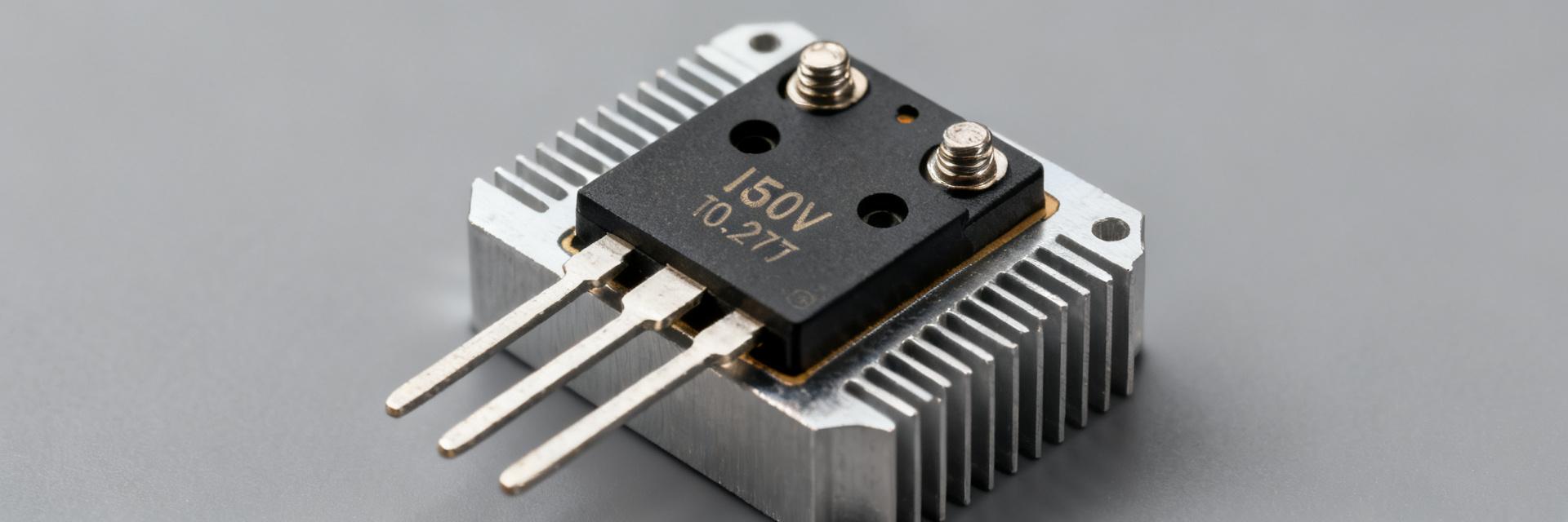
The module uses a press-fit/bolt-down power package with a flat baseplate and standardized high-current terminal layout; consult the datasheet mechanical drawings for mounting hole pattern, creepage distances and torque values. Board and layout engineers should confirm insulator thickness, required isolation gap for 1200 V, and follow recommended mounting torque and washer specs to avoid baseplate warpage and ensure repeatable thermal contact to the heat sink.
2 — Datasheet at a Glance: Key Electrical Specifications
Key datasheet sections to check immediately are the absolute ratings table, thermal resistances and switching characteristic charts. These define maximum Vce, continuous Ic, pulsed currents, Vces (emitter short-circuit), and VCE(sat) typical/maximum. Use stated Vce and Ic with safety margins—commonly 20–40% derating depending on cooling—to determine fit for a given application and expected ambient conditions.
| Parameter | Symbol | Min/Typ | Max | Unit |
|---|---|---|---|---|
| Collector-Emitter Voltage | VCES | - | 1200 | V |
| Continuous Collector Current | IC | - | 600 | A |
| Collector-Emitter Saturation Voltage | VCE(sat) | 1.8 | 2.2 | V |
| Gate-Emitter Threshold Voltage | VGE(th) | 5.5 | 7.0 | V |
| Junction Temperature | Tj | - | 175 | °C |
2.1 Static electrical ratings (Vce, Ic, Vces)
Locate Vce(max) = 1200 V and continuous current rating Ic in the static ratings table and verify pulsed current limits for short-duration transients. VCE(sat) typical and maximum values indicate conduction loss; use VCE(sat) × Ic to estimate conduction power loss. When validating, ensure the datasheet's test conditions (Tj, gate voltage, cooling) match your expected operating point to avoid underestimating losses.
2.2 Switching characteristics & dynamic losses
Switching tables list turn-on and turn-off times, Eon/Eoff energy per transition and di/dt limits. Map Eon and Eoff to your switching frequency to estimate switching loss: Psw ≈ (Eon+Eoff) × fsw × number_of_devices. Watch di/dt and dv/dt ratings to size snubbers, gate resistors and to design stray inductance controls that prevent voltage overshoot or latch-up during fast transitions.
3 — Thermal, Reliability & Limiting Parameters
Datasheet thermal tables provide Rth(j‑c), Rth(c‑s) and Tj(max). Use these to size heat sinks and cooling for steady-state and transient loads. Compute junction temperature under load using junction rise equations and validate against SOA and thermal cycling limits. Proper interpretation of these thermal values is essential to avoid accelerated ageing or sudden failure in high-duty applications.
3.1 Thermal resistances and junction limits
Start with the simple steady-state formula: Tj = Ta + Pd × (Rth(j‑c) + Rth(c‑hs) + Rth(hs‑a)). Use Pd = conduction_loss + switching_loss. For example, estimate Pd from VCE(sat)×Ic + (Eon+Eoff)×fsw. Select a heat sink such that Tj remains below Tj(max) with required derating; validate with thermal imaging under representative load to confirm thermal path assumptions.
3.2 Reliability metrics and safe operating area (SOA)
Review short-circuit withstand time, SOA plots and thermal cycling specifications in the datasheet. SOA curves govern allowable Vce/Ic combinations for specified pulse durations; margin these curves for lifetime and worst-case hot junctions. Verify thermal cycling and power cycling limits in procurement tests to ensure module solder or bond wire fatigue is acceptable for the intended mission profile.
4 — Integration & Test Guide: Gate Drive, Mounting, and Measurement
Integration success depends on proper gate drive, low-stray-inductance layout and controlled thermal interfaces. The datasheet gives recommended gate-emitter voltages and gate resistor ranges; follow those as starting points and tune gate resistance to trade off switching speed versus overshoot. Include desaturation detection and robust Miller clamp strategies for safe operation under short-circuit events.
4.1 Gate drive and protection recommendations
Design gate drive to match recommended Vge(on)/Vge(off) windows and account for gate threshold spread. Use Kelvin gate and emitter connections where provided, place gate resistors close to the gate terminal, and estimate loop inductance to limit dv/dt induced gate currents. Implement desat protection and a controlled active clamp to protect the device during overcurrent or extreme dv/dt events.
4.2 Mounting, cooling, and validation tests
Follow datasheet mounting torque and insulator guidance, use high‑conductivity TIM with controlled bondline thickness, and mechanically secure fasteners to spec. For incoming inspection, verify VCE(sat) at a defined test current, capture switching waveforms at rated gate drive, and perform temperature mapping across the baseplate under representative load to confirm thermal design assumptions and detect thermal hotspots early.
5 — Selection Checklist & Practical Application Examples
A structured checklist simplifies procurement: confirm voltage/current ratings with margin, compute switching losses at target frequency, verify Rth and cooling plan, check SOA for intended pulse profiles, confirm gate-drive compatibility and ensure you have the correct package suffix. Watch for package variants and suffix codes that change thermals or terminal layouts.
5.1 Quick selection checklist before procurement
Before ordering, ensure these items are validated against the datasheet: (1) Vce and continuous Ic with margin; (2) Eon/Eoff and estimated switching loss at fsw; (3) Rth and cooling capacity; (4) SOA curves matching pulse durations; (5) gate‑drive voltage and protection compatibility. Request the latest datasheet revision and confirm mechanical drawing revision for mounting fit.
5.2 Short application scenarios and configuration examples
Scenario A: 50 kW inverter switching at 10 kHz — compute conduction and switching losses, size heat sink to keep Tj below limit with airflow margin, and verify SOA for continuous PWM duty. Scenario B: traction drive with high peak currents — prioritize SOA margin, short‑circuit withstand capability and a conservative gate drive to limit di/dt. For each, validate with thermal cycling and full‑load waveform capture.
Summary
- Verify static and dynamic ratings in the datasheet: confirm Vce, Ic and VCE(sat) against expected operating points to avoid underestimating conduction losses for the IGBT Module.
- Calculate thermal budget using Rth values and expected Pd; design heat sink and TIM so junction temperature stays below Tj(max) under worst-case ambient and duty cycle.
- Validate switching behavior and SOA: estimate switching losses at your frequency, tune gate resistance for dv/dt control, and confirm short‑circuit and thermal cycling margins before integration.
Frequently Asked Questions
What key datasheet tables should I check first for MIF600R12C2TL-BP?
Start with the absolute ratings and thermal resistance tables, then the switching characteristics and SOA graphs. These sections give the limits for Vce, Ic, VCE(sat), Rth(j‑c), Eon/Eoff and short‑circuit withstand—crucial inputs for loss, cooling and protection calculations during design validation.
How do I estimate cooling needs from the datasheet for MIF600R12C2TL-BP?
Compute device power loss (Pd = VCE(sat)×Ic + (Eon+Eoff)×fsw), then use Tj = Ta + Pd×(Rth(j‑c)+Rth(c‑hs)+Rth(hs‑a)) to solve for required heat‑sink thermal resistance. Validate with thermal imaging under representative load to ensure hotspot control and to confirm TIM selection and mounting torque effectiveness.
What gate-drive protections are recommended for MIF600R12C2TL-BP?
Use a gate drive that enforces recommended Vge(on)/Vge(off) levels, place gate resistors close to the terminal, implement desaturation detection and a Miller clamp or active clamping for short‑circuit protection. Aim to limit di/dt with gate resistance and stray inductance control while balancing switching loss and voltage overshoot.
Is the MIF600R12C2TL-BP suitable for traction inverters?
Yes, its 1200V blocking capability and 600A current rating make it well-suited for medium-voltage traction stages, provided that derating for ambient temperature and vibration-resistant mounting protocols are strictly followed.