MPMT1002QT0 Full Specs & Performance Report for SMT
The MPMT1002QT0 delivers precision in compact SMT packages: typical TCR ~5 ppm/°C, power per element 125 mW (deratable), and operating temperature range −55°C to +155°C, making it relevant for high-accuracy sensor front-ends. This article analyzes full electrical and thermal specs, production test methods, and placement guidance to help PCB designers, process engineers, and procurement teams evaluate SMT performance and assembly risk for the MPMT1002QT0.
Readers will find actionable test procedures, derating guidance, and a production checklist tailored to thin film resistor networks used in precision voltage dividers and measurement circuits. The report emphasizes SMT performance metrics designers should request from vendors and the PCB-level checks that minimize drift and field failures.
1 — Why MPMT1002QT0 Matters for SMT Assemblies
1.1 Component class & primary applications
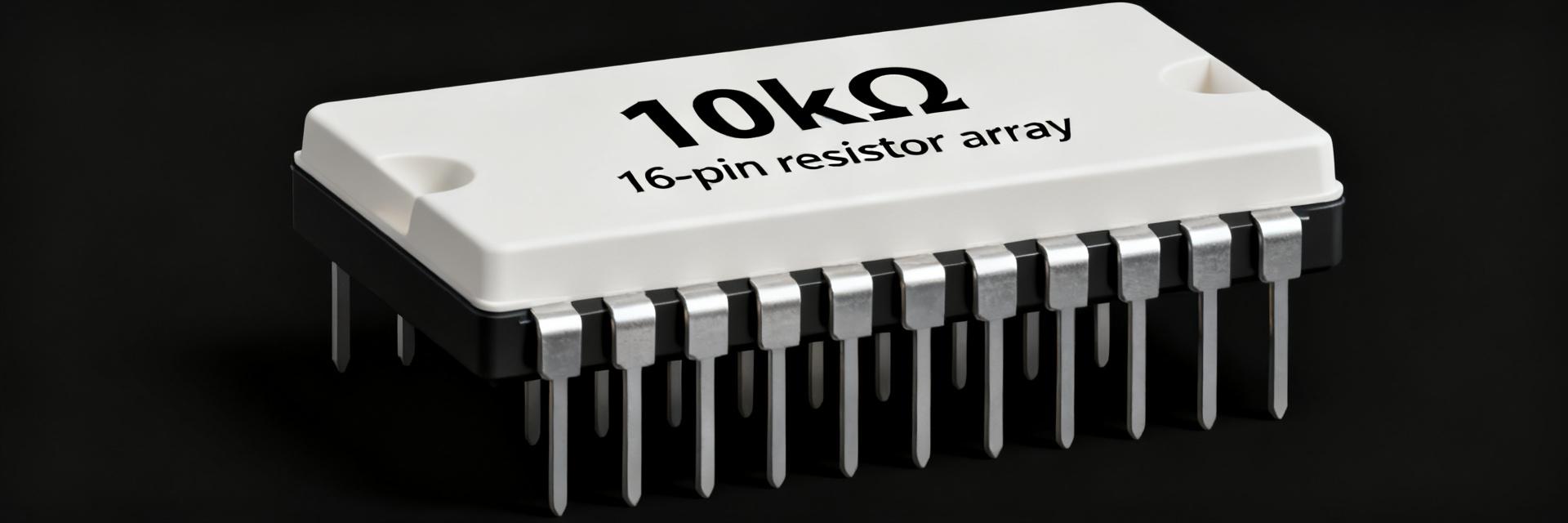
Point: MPMT1002QT0 is a multi-element thin film resistor network optimized for precision SMT use. Evidence: thin film resistor construction yields low TCR and tight stability versus thick-film alternatives. Explanation: designers use these networks in voltage dividers, sensor front-ends, and matched resistor arrays where ratio stability and low noise matter.
- Footprint: compact network package suitable for 0805-equivalent arrays
- Pin count: multi-terminal array (common configurations 4–8 terminals)
- Body size: small body height to fit low-profile assemblies
1.2 Key electrical & environmental specs at a glance
Point: Quick spec snapshot helps part selection. Evidence: core specs designers request include resistance values, tolerance, TCR (ppm/°C), power per element, and operating temperature range. Explanation: the table below provides a compact reference for PCB layout and thermal planning.
| Spec | Typical / Range |
|---|---|
| Resistance values | 10 Ω – 200 kΩ (array-dependent) |
| Tolerance | ±0.1% to ±1% |
| TCR | ~5 ppm/°C (typical) |
| Power per element | 125 mW (deratable with board temp) |
| Operating temp | −55°C to +155°C |
2 — Full Electrical Specs & What They Mean for SMT Performance
2.1 Resistance, tolerance, TCR and their PCB-level impact
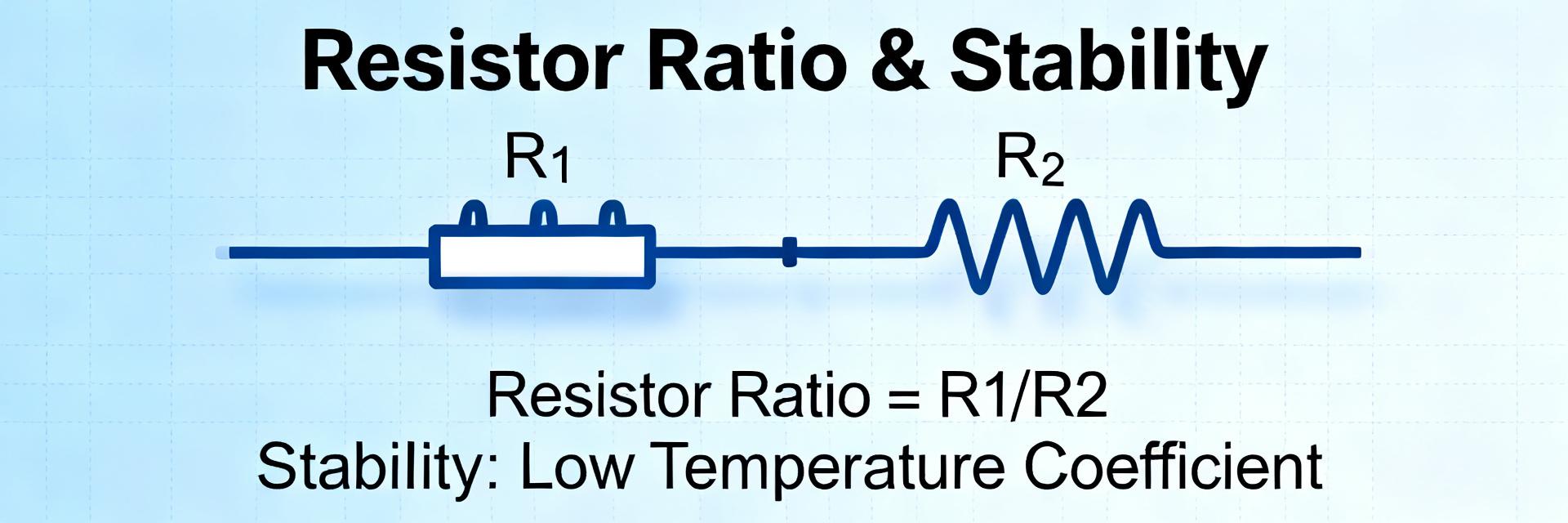
Point: Resistance range and tolerance directly set circuit accuracy; tight tolerances reduce calibration effort. Evidence: a ±0.1% divider resistor yields <0.2% error in a two-resistor divider compared with ±1% parts generating up to 2% error. Explanation: TCR expressed in ppm/°C governs temperature-induced drift; at 5 ppm/°C a 10 kΩ resistor changes ~0.05% per 100°C, critical for precision ADC front-ends and reference networks when board temperature varies.
2.2 Power handling, noise, and stability implications
Point: Small SMT networks exhibit limited dissipation per element; derating is required. Evidence: 125 mW element power in-board will be reduced at elevated board temps; thermal coupling affects neighboring components. Explanation: designers should compare power-per-element and long-term drift figures—low noise thin film resistors favor low-ppm stability in measurement chains, while poor derating leads to accelerated tolerance shifts and elevated noise over life.
3 — Thermal & Reliability Data: Reflow, Power, and Long-Term Drift
3.1 Reflow compatibility and thermal derating guidance
Point: Reflow survivability and thermal derating determine yield and in-field stability. Evidence: thin film networks tolerate standard lead-free reflow peak temperatures when recommended profiles are observed; excessive peak or extended dwell can affect adhesion or element stress. Explanation: use a conservative profile with max board temp below the package stress threshold and apply derating rules such as reducing allowable steady-state power by 50% for board temps above 85°C.
3.2 Reliability metrics, failure modes, and life-test expectations
Point: Common failure modes include tolerance shift and opens after severe thermal/humidity stress. Evidence: accelerated life tests for thin film arrays often show small ppm/√hr drift when properly qualified; missing supplier drift data is a red flag. Explanation: request humidity, thermal cycle, and power-soak reports; acceptance criteria for production qualification should include max drift limits (e.g., <0.1% shift after defined cycles) and no open circuits post-stress.
4 — How to Test MPMT1002QT0 in SMT Production
4.1 PCB-level electrical test procedures
Point: Accurate PCB-level testing prevents escapes and ensures performance. Evidence: four-wire Kelvin measurements remove lead resistance and are essential for precision values under 1 kΩ. Explanation: recommended flow: post-reflow visual → in-circuit resistance checks → selective four-wire verification for precision nodes. Establish fixture limits based on tolerance and expected drift; flag assemblies exceeding tolerance for rework.
4.2 Environmental & accelerated test checklist
Point: Accelerated tests confirm long-term behavior in the intended environment. Evidence: key tests include 85/85 humidity soak, thermal cycling (−55°C to +125°C cycles), and power-soak at elevated board temps. Explanation: measure resistances at predefined intervals (initial, mid, end) and use pass thresholds such as <0.1% change for critical networks; document failures (open, shift) and correlate to assembly processes.
5 — Assembly Scenarios & Placement Best Practices (Case Examples)
5.1 Typical use-case: precision voltage divider / sensor front end
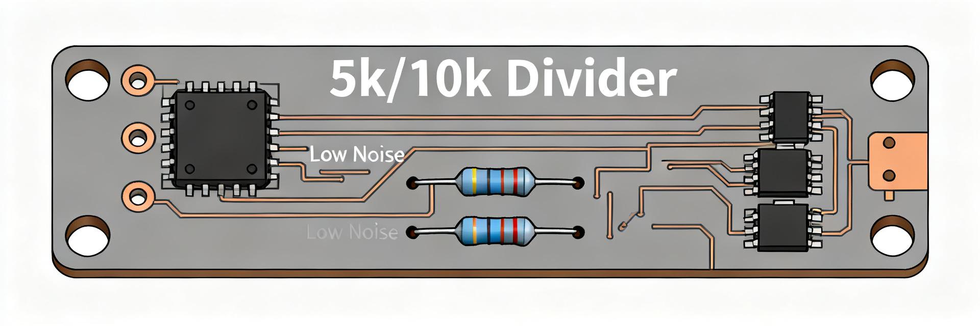
Point: A matched resistor array simplifies ratio stability in sensor circuits. Evidence: using a single network for both divider elements reduces drift from differential thermal stresses. Explanation: place the array close to the sensor or ADC input, align orientation to minimize thermal gradients, and route low-noise traces with ground returns to preserve measurement fidelity; expect improved calibration stability versus discrete unmatched parts.
5.2 High-density SMT layouts and pick-and-place considerations
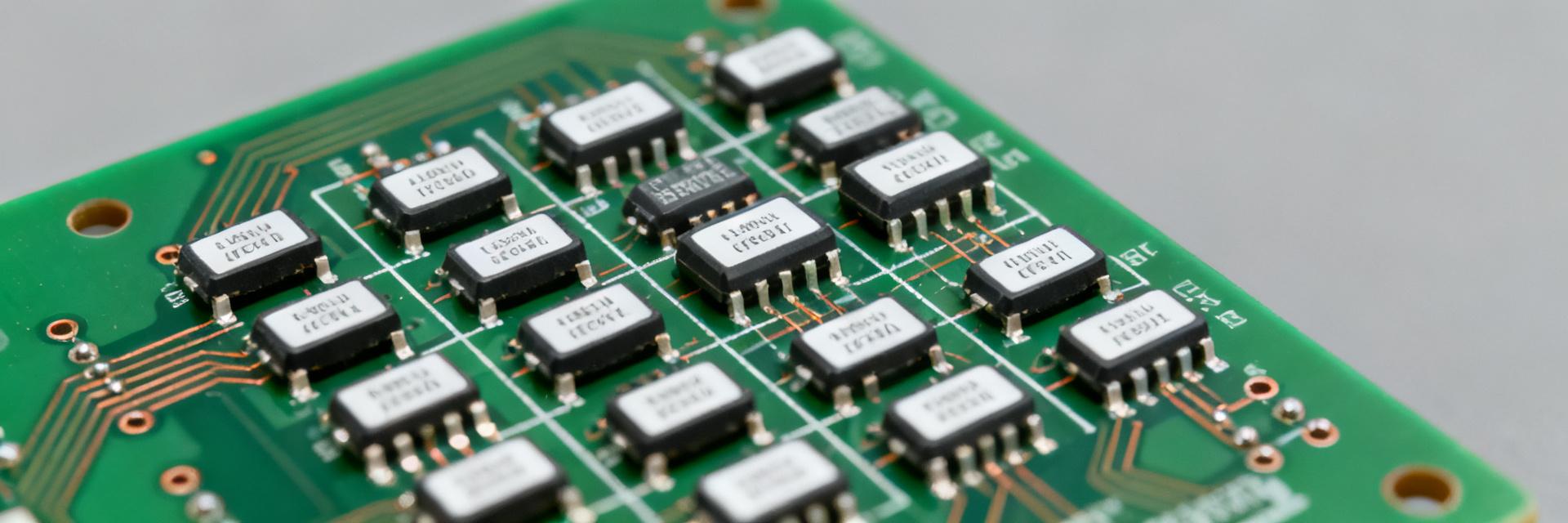
Point: Pick-and-place and reflow realities influence yields for small arrays. Evidence: tombstoning risk is low for multi-terminal networks but pad design and stencil volumes remain critical. Explanation: use appropriate nozzle selection, ensure secure feeder programming, apply controlled paste volumes, and adopt pad shapes that minimize uneven wetting; validate with pilot runs focusing on placement accuracy and solder fillet quality.
6 — SMT Design & Procurement Checklist for Using MPMT1002QT0
6.1 Design checklist: footprints, thermal relief & grounding
Point: DFM checks catch common assembly pitfalls. Evidence: recommended validations include footprint-to-datasheet dimension checks, pad expansion for reliable solder fillets, and thermal relief for heat-sensitive neighbors. Explanation: validate soldermask clearance, keep sensitive networks away from high-power components, and define thermal vias only when necessary to control board-local heat that affects SMT performance.
6.2 Procurement & vendor data to request before production
Point: Supplier data determines qualification confidence. Evidence: request lot-level TCR data, power/derating curves, reflow survivability, and sample drift reports. Explanation: red flags include missing TCR or environmental data; require pilot-run reports, incoming inspection criteria, and documented acceptance thresholds to ensure consistent SMT performance with the MPMT1002QT0.
Conclusion / Summary
The MPMT1002QT0 provides low-TCR, tight-tolerance thin film performance in a compact SMT format, making it a strong candidate for precision measurement and sensor front-end circuits. Top specs impacting SMT performance are TCR, power-per-element with derating rules, and documented long-term drift under expected environmental stress. Teams should run the PCB-level tests described and require supplier life-test data before production.
Next steps: validate footprint and reflow profile on a pilot panel, perform four-wire verification on critical nets, and secure lot-level TCR and power-derating reports from the supplier to lock in acceptance criteria for incoming inspection and qualification.
Key Summary
- MPMT1002QT0 delivers low TCR and tight tolerance suitable for precision SMT applications; verify resistance range and tolerance against required accuracy before layout (MPMT1002QT0, thin film resistor).
- SMT performance hinges on power-per-element derating and reflow compatibility; reduce allowable power at elevated board temperatures and use conservative reflow profiles to avoid package stress.
- Production qualification must include four-wire resistance checks, humidity and thermal cycling, and documented drift limits; missing vendor drift data is a procurement red flag.
Common Questions and Answers
What is the typical TCR for MPMT1002QT0 and how does it affect SMT performance?
Typical TCR for this class of thin film network is around 5 ppm/°C. Lower TCR reduces temperature-induced resistance changes, improving measurement stability across operating temps. For SMT performance this means lower calibration drift and tighter ratio stability in voltage dividers and sensor inputs.
How should a production line test MPMT1002QT0 arrays after reflow?
Use a two-step approach: quick in-circuit resistance checks to catch gross opens/shorts, followed by selective four-wire Kelvin measurements on critical nodes to verify precision values. Include test limits based on part tolerance and expected assembly-induced shifts to decide pass/rework criteria.
Which derating rules apply to MPMT1002QT0 power per element in high-board-temperature environments?
Apply conservative derating: reduce steady-state power allowance substantially at board temps above ~85°C (for example, 50% reduction). Account for thermal coupling from nearby components and validate with power-soak tests to ensure no excessive drift or failures during extended operation.
What are the typical SMT failure modes for MPMT1002QT0?
Common failure modes include resistance value drift and open circuits under extreme thermal shock or high humidity. These are minimized by applying correct thermal derating and verifying post-reflow solder joint integrity.