SOMC160310K0GRZ Complete Datasheet: Electrical Specs
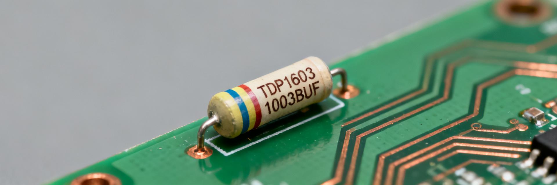
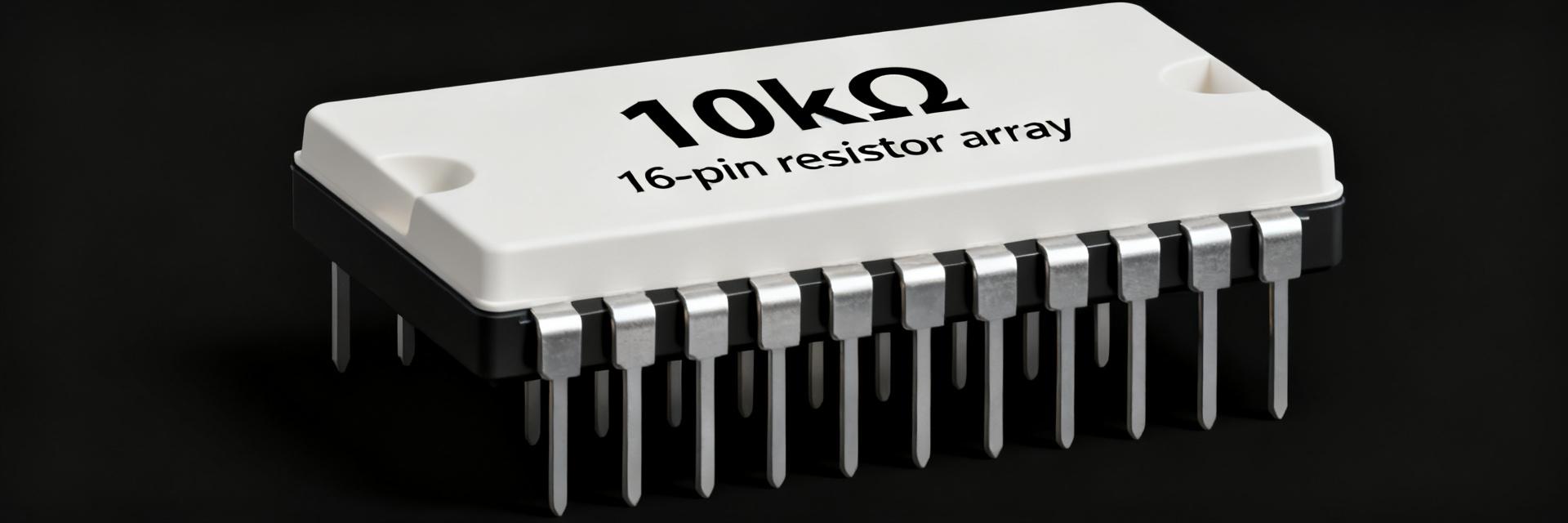
According to the SOMC160310K0GRZ datasheet, this eight‑resistor network is specified as 10 kΩ ±2%, 160 mW power per element, and 100 ppm/°C TCR in a 16‑pin dual‑in‑line package—electrical specs that make it suitable for compact divider arrays and multi‑channel pull‑ups. This introduction summarizes the most relevant electrical numbers and why they matter for board designers and system accuracy.
Key electrical specs and practical limits drive layout, thermal margin and test methods. This guide breaks down the numbers from the current datasheet, reconciles voltage vs. power limits, and gives concrete selection, layout and test guidance engineers can apply directly during validation and production.
1 — Product overview & quick electrical summary (background)
1.1 Quick-specs table (must-have numbers)
| Parameter | Typical / Nominal | Absolute / Max | Units / Notes |
|---|---|---|---|
| Resistance (per element) | 10 kΩ | — | Ω (datasheet) |
| Tolerance | ±2% | — | (datasheet) |
| Power rating (per element) | 160 mW | — | mW (datasheet) |
| TCR | 100 ppm/°C | — | ppm per °C (datasheet) |
| Max voltage (absolute) | — | 50 | V (datasheet) |
| Package / pins | 16‑pin dual‑in‑line | — | DIP / SIP family (datasheet) |
| Operating temp | −55 to +155 | — | °C range (datasheet) |
| Isolation between elements | Specified per datasheet | — | Resistance to adjacent elements (datasheet) |
1.2 Package & pinout overview
The network is supplied in a 16‑lead dual‑in‑line package with standard 0.1‑inch lead spacing; pin assignments place resistor ends on adjacent pins across the package body. Mechanical tolerances and pin‑to‑pin isolation values are listed in the datasheet; designers should reference the recommended PCB footprint and maintain consistent solder fillets and thermal reliefs to avoid mechanical stress or thermal coupling between elements.
2 — SOMC160310K0GRZ datasheet — Detailed electrical specifications (data analysis)
2.1 Resistor element characteristics
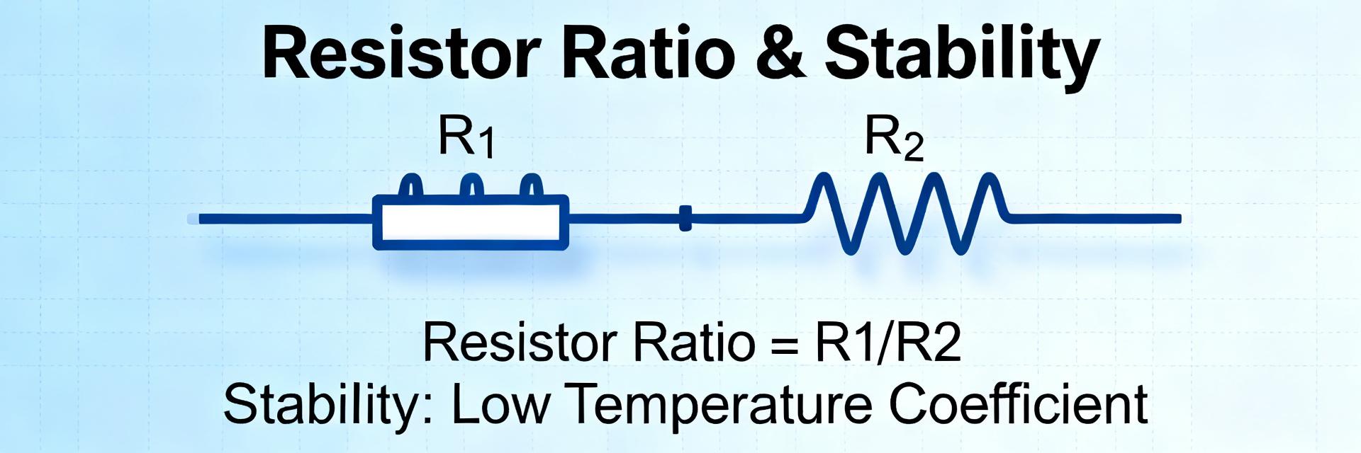
Resistance tolerance ±2% sets nominal matching; TCR of 100 ppm/°C means a 10 kΩ element shifts ~1 Ω per 1°C change. Power limits and voltage constraints interact: use P = V² / R and Vmax_power_limited = sqrt(P_rating × R). For 10 kΩ at 160 mW: Vmax_power_limited ≈ sqrt(0.16 × 10000) = 40 V, below the datasheet absolute‑max voltage of 50 V. The difference reflects separate constraints—steady‑state power dissipation vs. dielectric/flashover limits—so both must be respected in designs.
2.2 Operating/environmental and reliability specs
The current datasheet lists wide operating temperatures (down to −55 °C and up to +155 °C) and soldering/reflow profiles for reliability. Thermal resistance and derating information are provided; read derating curves to shift allowable continuous power at elevated ambient temperatures. Storage and mechanical shock specs guide handling: follow recommended solder profiles to avoid resistance shifts from thermal stress.
3 — Performance characterization & test guidance (data analysis / method)
3.1 Typical performance graphs & what to expect
Datasheet graphs typically show resistance vs. temperature, long‑term stability and short‑term drift. Expect tens to hundreds of ppm drift over thousands of hours depending on mounting and ambient. For ADC or sensor references, translate ppm drift into LSB error at the system ADC range; use the resistance vs. temperature curve to predict worst‑case offset across the operating range and add margin accordingly.
3.2 How the datasheet tests specs (measurement methods)
Typical test methods include four‑wire (Kelvin) resistance measurement, defined test voltages/currents, and thermal soak to stabilize readings. For validation, measure each element with a calibrated DMM or LCR meter, perform thermal step tests, and record drift after reflow. A practical test checklist: 4‑wire DC resistance, power dissipation test at expected current, thermal cycling and post‑reflow resistance comparison against datasheet limits.
4 — Application guidelines & circuit examples (methods / case)
4.1 Typical application circuits and layout tips
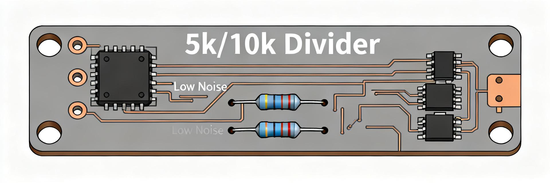
Common uses: multi‑channel pull‑ups, resistor ladder for ADC reference, and input termination arrays. Example schematic snippet for a 4‑channel pull‑up: each element from IO pin to VCC. Layout tips: group network close to the IO header, match trace lengths for ladder accuracy, and provide thermal relief to prevent power dissipated in one element from heating adjacent elements and skewing values.
4.2 Thermal management, derating calculations & safety margin examples
Derating example: with 160 mW rating and board conditions that reduce dissipation capability, target 50% margin for continuous loads → allowable per element ≈80 mW. If element dissipates P_expected = V²/R, solve for V: V_allowed = sqrt(P_allowed × R). For 10 kΩ and 80 mW, V_allowed ≈ sqrt(0.08×10000)=28.3 V. Always check both power‑limited and absolute voltage limits.
5 — Selection checklist, troubleshooting & procurement notes (action)
5.1 Quick selection checklist
- Confirm required resistance & tolerance match the network nominal value and tolerance.
- Verify power per element plus margin (recommend ≥50% for continuous use) against expected dissipation.
- Check TCR requirement for temperature sensitivity and system accuracy needs.
- Confirm package/pinout fits board footprint; review datasheet mechanical drawing before layout.
- Red flags: dissipation near rating, high ambient temp, or pinout mismatch.
5.2 Common issues and fixes (troubleshooting)
Typical problems include post‑reflow resistance shift (solder stress), thermal coupling causing element-to-element drift, and measurement errors from two‑wire methods. Fixes: use four‑wire measurements, add thermal barriers or spacing between dissipating elements, follow recommended reflow profile, and replace suspect parts showing out‑of‑spec drift. When isolating faults, test the component off‑board to separate board vs. part issues.
Summary (conclusion & call to action)
- The SOMC160310K0GRZ electrical specs—10 kΩ ±2%, 160 mW/element and 100 ppm/°C TCR—define suitability for compact divider arrays and pull‑up banks and set thermal and accuracy constraints.
- Power vs. voltage limits must both be checked: use P = V²/R and Vmax_power_limited = sqrt(P_rating × R) and then reconcile with the absolute voltage in the datasheet.
- Layout and thermal management (spacing, thermal reliefs, derating margins) directly impact long‑term stability and measurement accuracy in ADC or sensor front‑ends.
Engineers should consult the current datasheet for final confirmation of pack, mechanical and electrical figures before finalizing layouts or procurement; verify power margins and perform four‑wire validation on assembled boards to ensure conformance.
6 — Common questions
What are the typical power and voltage limits for SOMC160310K0GRZ?
Per the datasheet the per‑element continuous power rating is 160 mW and the absolute voltage limit is listed as 50 V. For steady‑state operation use the power‑limited voltage calculation V = sqrt(P_rating×R) to avoid exceeding dissipation even when absolute‑voltage appears permissible.
How does TCR affect precision applications using this resistor network?
A TCR of 100 ppm/°C implies noticeable drift over large temperature swings: for 10 kΩ, a 50 °C change yields ~5000 ppm (0.5%) shift if unmitigated. For precision ADC references, compensate by design (temperature compensation, calibration, or selecting tighter TCR) or by limiting operating temperature swings.
What test steps should be included to validate SOMC160310K0GRZ on a populated board?
Validation steps: four‑wire resistance baseline, post‑reflow comparison, thermal soak and step tests, and powered stress at expected application voltage with monitoring. Record deviations vs. the datasheet claims and ensure margins for continuous dissipation and ambient temperature are maintained.
How do you layout the SOMC160310K0GRZ to prevent thermal coupling?
To prevent thermal coupling and drift, group the network close to the IO header, match trace lengths for ladder accuracy, and provide physical spacing or thermal barriers between dissipating elements. Standard thermal reliefs should be used on all pin footprints.