


Helping you save cost and time.

Provide reliable packaging for your goods.

Quick and reliable delivery to save time.

Excellent after-sales service.
New Product Launch
More +


Hot Selling Parts


Blog

Part Number Lookup: Latest Search Insights & Data Trends
Recent search telemetry and marketplace analytics show a clear acceleration in queries tied to part number lookup, driven by tighter supply chains, improved mobile access, and fitment-aware discovery.…
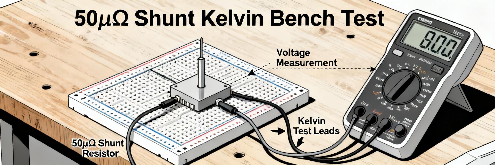
HoFL3-8436-A-50uR-1 shunt resistor datasheet & tests
Lab samples of a 50 μΩ shunt typically show R ≈ 50 μΩ ±1% at room temperature, a TCR on the order of 50–150 ppm/°C, and a 2.5 mV voltage drop at 50 A; this article summarizes measured expectations for…
Current Sense Resistor 250 µΩ: Performance Specs & Datasheet
2026-07-21 09:59:18
100µΩ shunt resistor datasheet: measured specs & charts
2026-07-20 10:00:23
100µΩ shunt resistor: Full specs & measured data report
2026-07-19 09:59:17
HoFL3-8536 25µΩ 0.5% Shunt Resistor: Measured Specs
2026-07-18 10:04:16
HoFL3-8436-B 50µΩ Shunt: Complete Performance Datasheet
2026-07-17 10:05:17
Read more