


Helping you save cost and time.

Provide reliable packaging for your goods.

Quick and reliable delivery to save time.

Excellent after-sales service.
New Product Launch
More +


Hot Selling Parts


Blog
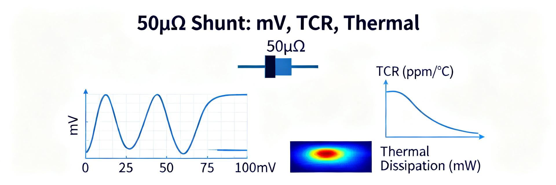
HoFL3-8536 50µΩ 50W Shunt: Data-Driven Test Report
Point: This report consolidates controlled lab measurements to quantify how a 50µΩ, 50W shunt behaves under realistic electrical and thermal stress. Evidence: Measured metrics include DC resistance, t…

Part Number Lookup: Latest Search Insights & Data Trends
Recent search telemetry and marketplace analytics show a clear acceleration in queries tied to part number lookup, driven by tighter supply chains, improved mobile access, and fitment-aware discovery.…
HoFL3-8436-A-50uR-1 shunt resistor datasheet & tests
2026-07-24 09:58:17
HoFL3-8536 100µΩ Shunt: Measured Specs & PCB Tips Guide
2026-07-23 09:58:16
HoFL3-8536 Shunt Resistor: Latest Measured Report & Analysis
2026-07-22 09:59:17
Current Sense Resistor 250 µΩ: Performance Specs & Datasheet
2026-07-21 09:59:18
100µΩ shunt resistor datasheet: measured specs & charts
2026-07-20 10:00:23
Read more