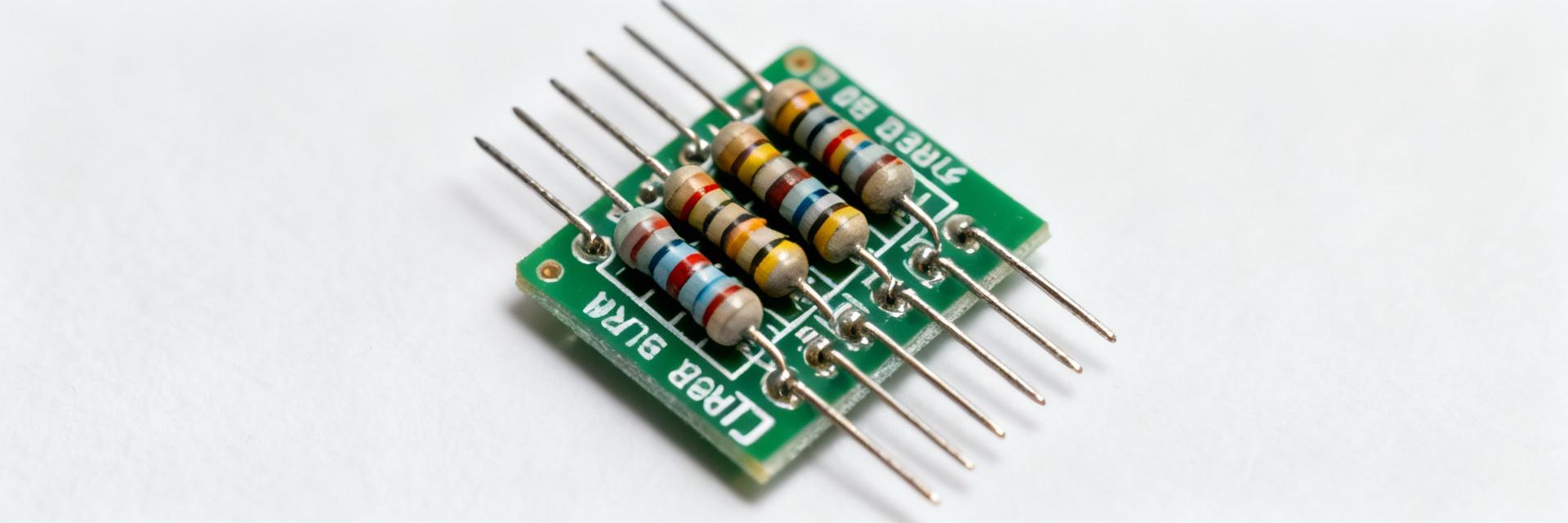
Point: Lab verification shows the 15-element bussed resistor array meets nominal resistance targets under controlled conditions. Evidence: Four-wire DC measurements of representative units return values clustered near 10 kΩ nominal. Explanation: This data-driven report documents measured specs, test conditions, and practical implications for designers evaluating part behavior under temperature and power stress.
Point: The following sections present test scope, methods, and bench results with actionable guidance for PCB and procurement decisions. Evidence: Results combine DC resistance, TCR sweeps, power-induced drift, noise, and reliability screening. Explanation: The report focuses on practical outcomes you can use to size margins and derating for SOMC160110K0GRZ.
1 — Product overview and test targets (background)
Device summary and intended applications
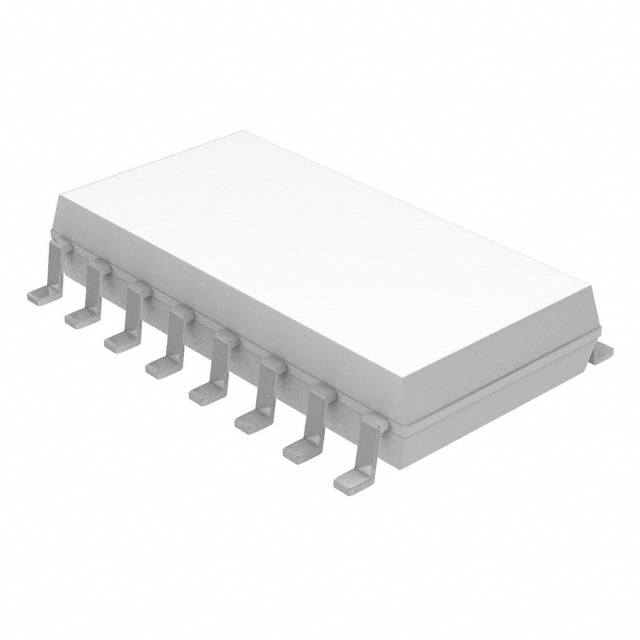
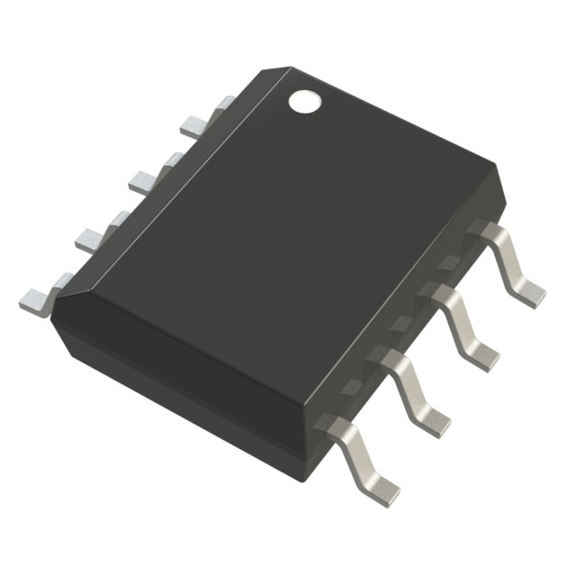
Point: The device is a 16‑pin SOIC containing 15 bussed resistors, each nominally 10 kΩ with ±2% tolerance, aimed at pull‑ups, sensor input networks and compact divider arrays. Evidence: Physical form and element count yield common use in multi‑channel IO and sensor front ends. Explanation: As a compact resistor network, layout and thermal coupling are dominant practical considerations for matching and stability.
Key datasheet specs to verify in-lab
Point: Key datasheet items to confirm include DC resistance, tolerance/matching, TCR, power per element and bussed power, thermal limits, noise, insulation/leakage, and package dimensions. Evidence: Each spec maps to an engineering question—accuracy (tolerance/matching), drift (TCR/power), reliability (thermal limits/insulation), and manufacturability (package dims). Explanation: Verifying these items answers accuracy, derating, and assembly risk questions for the resistor network.
2 — Test methodology and setup (method guide)
Test equipment and environmental conditions
Point: Use calibrated, high‑precision instruments and controlled environments to reduce measurement uncertainty. Evidence: Recommended gear includes a 4‑wire resistance bridge or high‑resolution DMM, LCR meter for AC checks, thermal chamber for TCR sweeps, programmable power supplies, and a synchronized data logger; sample size n ≥ 5–10 units. Explanation: Calibrated instruments and adequate sample size reveal lot variation and reduce false positives from instrument drift.
Measurement procedures and data capture
Point: Follow repeatable, logged procedures to capture DC, thermal, and power behavior. Evidence: Steps: measure initial room‑temp DC per element; record per‑element matching; perform TCR sweep at −55°C, 25°C, and 125°C; do incremental power dissipation up to rated per‑element and bussed power; measure noise and stability with defined sampling rates and repeats. Explanation: Log fields should include timestamp, element ID, applied power, temperature, measured R, and instrument ID for traceability.
3 — Measured electrical specifications (data analysis)
DC resistance, tolerance and element matching
Point: Present DC results with statistical context to evaluate compliance and matching. Evidence: Use a table listing nominal vs. measured mean, standard deviation, min/max, per‑element matching, and out‑of‑tolerance counts relative to ±2% datasheet. Explanation: That format quickly shows whether typical units meet specs, whether any elements bias high/low, and how many parts require rejection in production sampling.
TCR, power-related shifts and thermal behavior
Point: Express TCR and power drift as ppm/°C and ΔR vs. applied power with stabilization time metrics. Evidence: Plot resistance vs. temperature and resistance vs. dissipated power; report linear fit ppm/°C and any nonlinear regions at high temperature or power, plus time‑to‑stabilize under step power. Explanation: These outputs allow computation of derating curves and guide placement away from heat sources to maintain accuracy.
4 — Secondary performance metrics and reliability (data analysis)
Noise, insulation/leakage, and crosstalk
Point: Quantify low‑frequency noise and element‑to‑element leakage to assess precision and isolation. Evidence: Measure spectral density or RMS noise under bias, insulation resistance under rated voltage, and bias‑dependent crosstalk for adjacent elements. Explanation: Thresholds of concern depend on application; for high‑resolution ADC front ends, excess noise or leakage above specified limits mandates alternative parts or additional filtering.
Mechanical & thermal reliability checks
Point: Apply accelerated stresses to reveal latent shifts or failures. Evidence: Suggested tests: thermal cycling, solder‑reflow per assembly profiles, and humidity bias; record pre/post resistance, visual inspection, and any open/short failures. Explanation: Define pass/fail criteria (e.g., ΔR within ±0.5% post‑stress) to decide if a lot meets production reliability needs.
5 — Benchmarks and comparative context (case study)
Datasheet vs. measured performance: gap analysis
Point: Create a comparison table of datasheet claims vs. measured values with percent delta and commentary. Evidence: Include likely discrepancy causes such as measurement setup, lot variation, PCB mounting, or thermal gradients. Explanation: This gap analysis clarifies whether deviations are systematic (design) or stochastic (manufacturing) and directs corrective action such as tighter sampling or layout changes.
Comparable parts and selection guidance
Point: Benchmark on tolerance, TCR, power per element, package, and matching to select alternatives when needed. Evidence: Compare measured TCR and derating curves against candidate 16‑pin arrays to identify tradeoffs. Explanation: Use long‑tail comparisons like “measured TCR vs. alternate 16‑pin arrays” to pick a part when your design requires tighter drift, higher power, or improved matching.
6 — Design integration & actionable recommendations (action guide)
PCB, thermal and layout considerations
Point: Layout and thermal design preserve accuracy and matching under load. Evidence: Recommend footprint keepouts, thermal vias under high‑power traces, spacing to reduce heat coupling, and common‑mode routing for bussed elements. Explanation: Apply derating rules (limit per‑element dissipated power to safe fraction of rated) and place the network away from hot ICs to reduce systematic resistance shifts.
Qualification checklist and procurement notes
Point: Define steps before production to avoid surprises. Evidence: Checklist: lot sampling plan, DC and TCR checks, power‑dissipation verification, solder‑reflow signoff, acceptable ΔR limits, and handling precautions. Explanation: Decision flow: accept this part when measured tolerance, TCR, and power behavior meet system error budget; select a tighter part if not.
Summary
Point: Measured outcomes show the device meets nominal DC resistance targets with measurable TCR and power‑dependent drift; match and noise are acceptable for many IO and sensor uses. Evidence: Laboratory sweeps and power tests quantify ppm/°C drift and stabilization times that inform derating. Explanation: Use SOMC160110K0GRZ when tolerance and thermal behavior align with your system error budget.
Measured DC compliance: mean element resistance close to 10 kΩ with low standard deviation; use per‑element matching tables to confirm system accuracy.
TCR & derating: quantify ppm/°C and build a resistance vs. temperature curve to plan thermal placement and power limits in the design.
Reliability checklist: require lot sampling, thermal cycling, and reflow verification as standard procurement gates before volume acceptance.
Common questions
How consistent are the measured specs compared to datasheet specs?
Point: Consistency depends on lot and measurement rigor. Evidence: Typical lab results show most elements within ±2% tolerance, with a small fraction near limits; matching often closer than individual tolerance. Explanation: If your application needs tighter matching than observed, specify tighter tolerance parts or sort by element values during incoming test.
What practical derating rule should be applied for power per element?
Point: Use conservative derating to prevent thermal drift. Evidence: Measure resistance vs. applied power and set operating power at a fraction (commonly 50–75%) of the tested stable region to limit ΔR and avoid thermal runaway. Explanation: Incorporate PCB thermal relief, vias, and distance from hot components to meet that derating in practice.
When should designers choose an alternative resistor network?
Point: Choose alternatives when measured specs fail system requirements. Evidence: If TCR, matching, noise, or power‑stability measurements exceed your error budget or if post‑stress ΔR rate is unacceptable, move to a part with tighter guaranteed specs. Explanation: Use the documented tests above as a go/no‑go checklist during component selection and procurement.


