HoFL3-8518-B Datasheet: 100µΩ Current Sense Analysis
The HoFL3-8518-B presents a nominal 100µΩ shunt optimized for ultra-low loss, high-accuracy measurement. This article translates the key datasheet entries into practical design and test guidance for US electrical engineers, focusing on how a 100µΩ choice impacts accuracy, thermal design, and measurement chain selection for reliable current sensing.
We will interpret electrical specs, show worked examples (10 A and 100 A), recommend four-wire test setups and PCB layout practices, and give a verification checklist so teams move from datasheet reading to validated prototype quickly and predictably.
1 — Why ultra-low (100µΩ) current sense matters (Background)
1.1 Principles of low-ohm current sensing
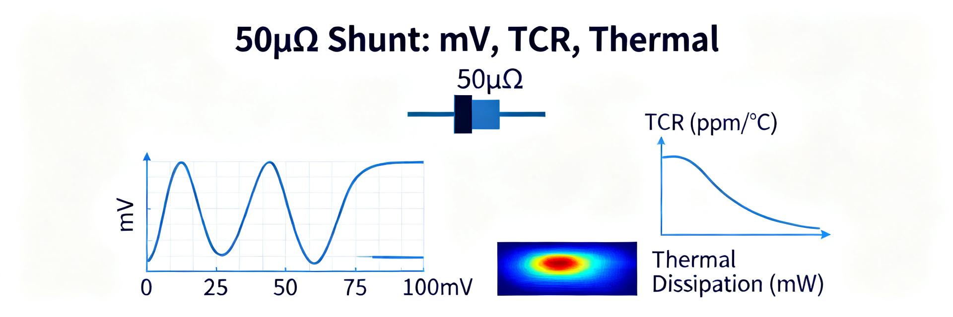
Shunt sensing converts current to voltage: V = I × R. With R = 100µΩ, V = 0.0001 × I. For 10 A, V = 1 mV; for 100 A, V = 10 mV. Power loss is P = I² × R → 10 A gives 0.01 W; 100 A gives 1 W. Low R minimizes loss but demands low-noise amplification and careful layout for resolution.
1.2 Key performance metrics to watch on any datasheet
Prioritize DC resistance (nominal and tolerance), TCR (ppm/°C), power rating, thermal time constant, offset and noise, and measurement bandwidth. Each spec affects accuracy: tolerance sets static scale error, TCR causes temperature-dependent gain change, and thermal time constant defines stabilization after current steps—read tables for test conditions.
2 — HoFL3-8518-B datasheet: electrical specifications decoded (Data analysis)
2.1 DC resistance, tolerance and what 100µΩ implies in system design
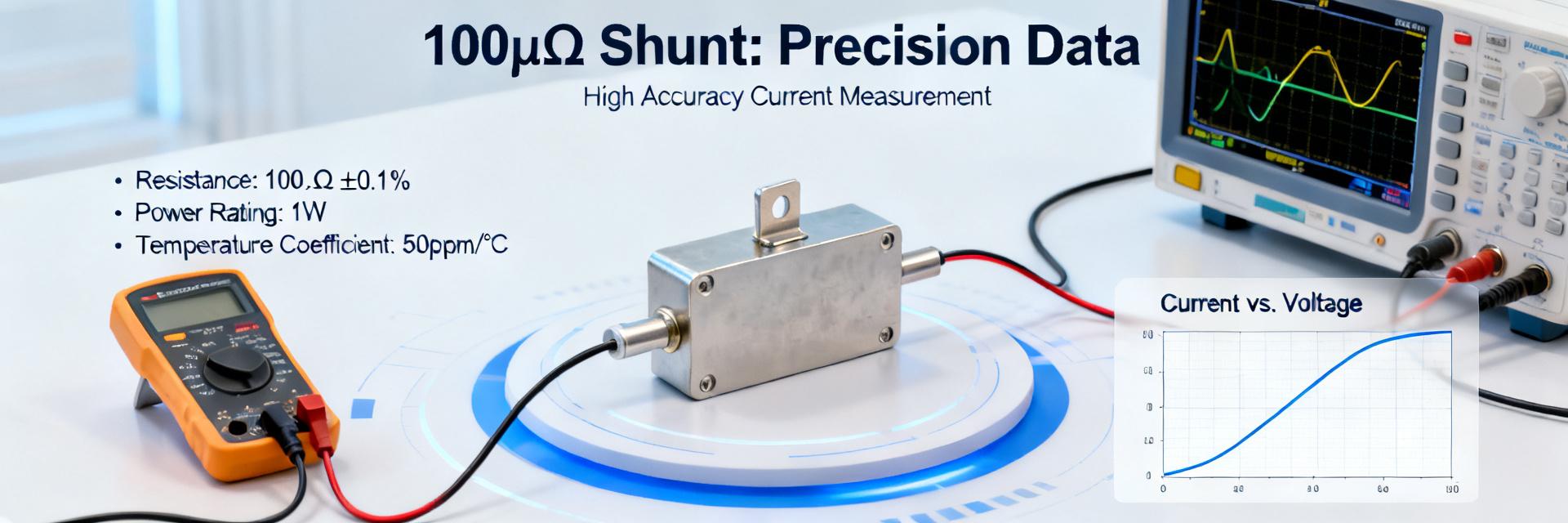
Convert resistance to mV/A: 100µΩ → 0.1 mV/A. Tolerance (e.g., ±0.5%) yields worst-case scale error ±0.5% before calibration. Example sensitivity: at 100 A the nominal drop is 10 mV; a ±0.5% tolerance is ±50 µV. In summary, HoFL3-8518-B-100uR-0.5% requires amplification to reach useful ADC range.
| Current (A) | Shunt Voltage Drop (V = I × R) | Power Dissipation (P = I² × R) | Min. Signal Amp Gain (for 1V FS) |
|---|---|---|---|
| 10 A | 1.0 mV | 0.01 W | 1000x |
| 50 A | 5.0 mV | 0.25 W | 200x |
| 100 A | 10.0 mV | 1.00 W | 100x |
2.2 Accuracy, offset, drift, and thermal behavior from the datasheet
Total system error = resistor tolerance + TCR × ΔT + amplifier offset/Gain error + ADC quantization/noise. Use error-budget equation: %Error_total ≈ sqrt(sum of squared contributors). Read drift tables to translate TCR (ppm/°C) into µV/°C at your operating current, then allocate margin in the amplifier and firmware calibration.
3 — Measuring a 100µΩ shunt: test setups and common error sources (Method guide)
3.1 Recommended bench setups: four-wire (Kelvin) measurement and PCB layout tips
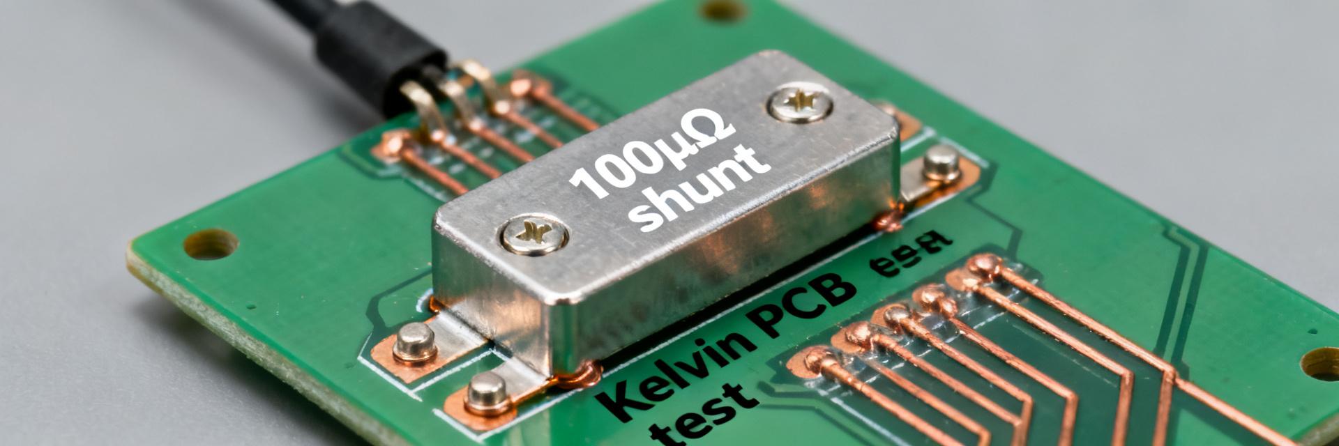
Use four-wire sense to remove lead resistance: force current through heavy traces and sense voltage with separate Kelvin pads and twisted pair to the amplifier. Keep sense wiring short, use guard traces, minimize loop area, and avoid routing sense traces under noisy power planes. For bench, use low-thermal EMF connectors and differential probes.
3.2 Noise, thermal EMF, and calibration strategies
Thermoelectric voltages can be tens of µV at junctions—comparable to shunt drops. Mitigate by using matched metals, isothermal layout, and reversing current tests. Calibrate with a traceable current source: record scale factor and temperature coefficient, store compensation coefficients in firmware, and average samples with appropriate bandwidth limiting to reduce noise.
4 — Practical design example: integrating HoFL3-8518-B in a power supply (Case study)
4.1 Schematic choices, ADC front-end and protection
For a 0–100 A range with 100µΩ, expect 0–10 mV raw. Choose an instrumentation amplifier (or dedicated sense amplifier) with low offset and gain ~100 to produce 0–1 V span. Include input RC filtering, common-mode protection, surge clamps, and a resistor-based divider or comparator for fast overcurrent detection to protect ADC and downstream electronics.
4.2 Simulation vs. bench: expected vs. observed performance
Simulate self-heating: 1 W at 100 A predicts temperature rise based on thermal resistance; use datasheet thermal time constant to estimate stabilization time. On bench, measure mV/A, drift per 10°C and compare to predicted TCR effects—e.g., 50 ppm/°C → 0.005% per 10°C producing ~0.5 µV at 10 mV nominal.
5 — Datasheet-driven checklist and next steps for engineers (Actionable recommendations)
5.1 Pre-prototype spec checklist
Before ordering, confirm DC resistance and tolerance variant availability, required TCR, continuous power rating, transient ratings, soldering/process limits, and environmental qualifications on the datasheet. Ask suppliers for test conditions and lot traceability if not listed. Note: HoFL3-8518-B-100uR-0.5% may have alternate tolerances—choose per calibration plan.
5.2 Verification, firmware handling and diagnostics
Implement factory calibration (measure known currents and store scale/offset), temperature compensation via lookup table or linear correction, and runtime diagnostics: periodic zero checks, drift alarms if scale deviates beyond threshold, and open-shunt detection using expected voltage vs. commanded current comparisons.
Summary
The HoFL3-8518-B’s 100µΩ rating drives a design trade-off: minimal power loss at the cost of sub-millivolt signals that demand low-noise amplification, careful PCB layout, and temperature compensation informed by the datasheet. From datasheet extraction to prototype, prioritize tolerance, TCR, thermal limits, and a clear calibration plan for accurate, repeatable current measurement.
Key summary
- 100µΩ gives 0.1 mV/A (10 A → 1 mV, 100 A → 10 mV); amplification and ADC planning are essential for resolution and headroom.
- Datasheet-driven checks: confirm resistance tolerance, TCR, power rating and thermal time constant to size cooling and calibration routines properly.
- Test and layout: use four-wire Kelvin sense, minimize thermoelectric junctions, and apply firmware temperature compensation and periodic self-tests for long-term accuracy.
Frequently Asked Questions
How do I interpret HoFL3-8518-B nominal resistance and tolerance for calibration?
Use the nominal 100µΩ and stated tolerance to compute scale factor (0.1 mV/A). Calibrate with a traceable current source to remove tolerance error, and store gain/offset in firmware. Include TCR correction from the datasheet to compensate temperature-induced gain shifts during operation.
What test setup ensures lowest measurement error for HoFL3-8518-B?
A four-wire Kelvin measurement with short sense leads, matched junction metals, guarded differential inputs, and reversing-current checks minimizes parasitic resistance and thermal EMFs. Use a low-noise amplifier and average as needed; document measurement bandwidth to match your application’s transient response.
Can firmware fully compensate HoFL3-8518-B drift and aging?
Firmware compensation (lookup tables, linear T correction, periodic recalibration) handles TCR and predictable drift. However, implement diagnostics to detect abrupt changes (open shunt or sudden drift) and schedule periodic hardware recalibration to account for long-term aging beyond firmware correction ranges.
What are the power dissipation and signal level implications at 10 A vs. 100 A?
Power loss is P = I² × R. At 10 A, the loss is just 0.01 W, while at 100 A, it reaches 1 W. Low resistance minimizes system power loss, but requires highly sensitive, low-drift amplifiers to accurately capture the resulting sub-millivolt voltage drops (1 mV at 10 A, 10 mV at 100 A).