


Helping you save cost and time.

Provide reliable packaging for your goods.

Quick and reliable delivery to save time.

Excellent after-sales service.
New Product Launch
More +


Hot Selling Parts


Blog
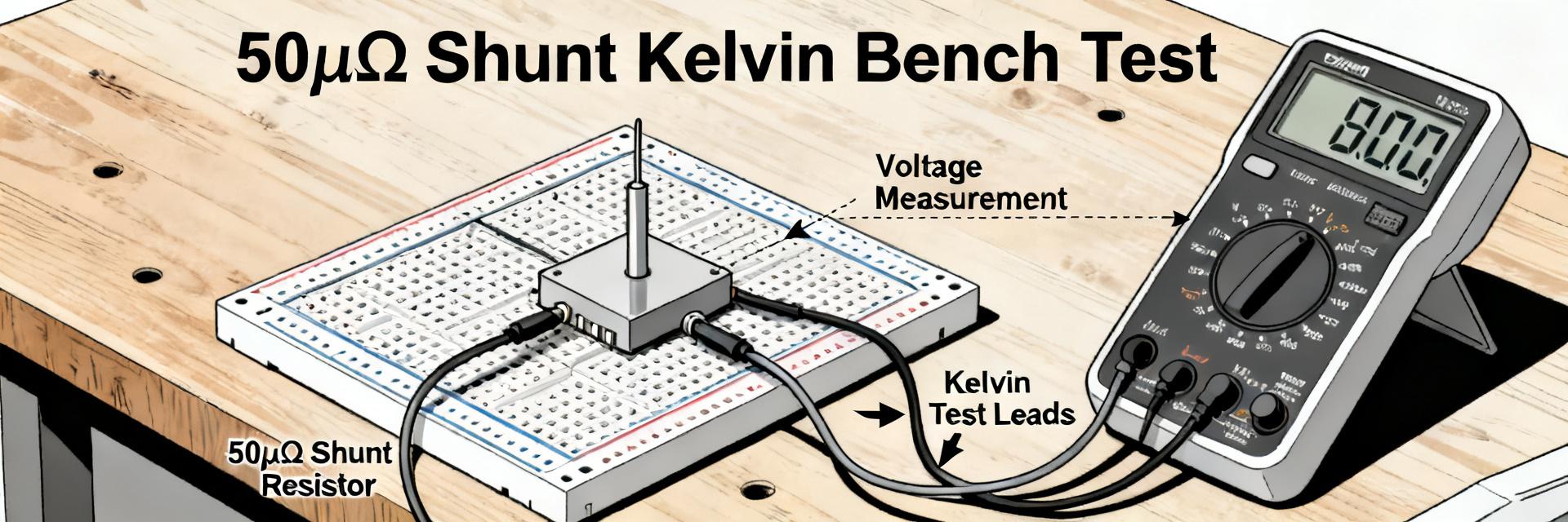
HoFL3-8436-A-50uR-1 shunt resistor datasheet & tests
Lab samples of a 50 μΩ shunt typically show R ≈ 50 μΩ ±1% at room temperature, a TCR on the order of 50–150 ppm/°C, and a 2.5 mV voltage drop at 50 A; this article summarizes measured expectations for…
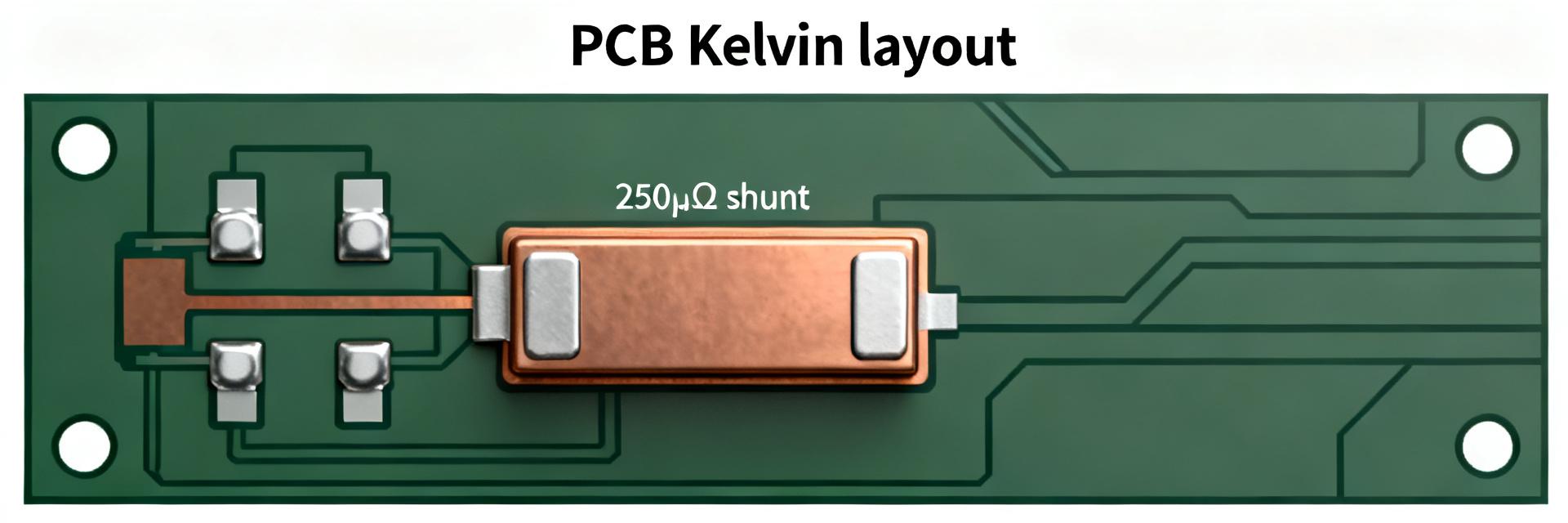
Current Sense Resistor 250 µΩ: Performance Specs & Datasheet
In many high-current systems a 250 µΩ resistor produces only 25 mV at 100 A but still dissipates 2.5 W—small voltages and significant heat make part choice and integration critical. This guide explain…
HoFL3-8536 25µΩ 0.5% Shunt Resistor: Measured Specs
2026-07-18 10:04:16
HoFL3-8436-B 50µΩ Shunt: Complete Performance Datasheet
2026-07-17 10:05:17
100 μΩ 0.5% Shunt Resistor: Bench Data, TCR & Noise
2026-07-16 10:06:16
HoFL3-8436-B shunt datasheet: key specs & test data
2026-07-15 10:05:15
HoFL3-8536 Shunt: Deep Lab Report on Accuracy & TCR
2026-07-14 10:38:18
Read more