


Helping you save cost and time.

Provide reliable packaging for your goods.

Quick and reliable delivery to save time.

Excellent after-sales service.
New Product Launch
More +


Hot Selling Parts


Blog
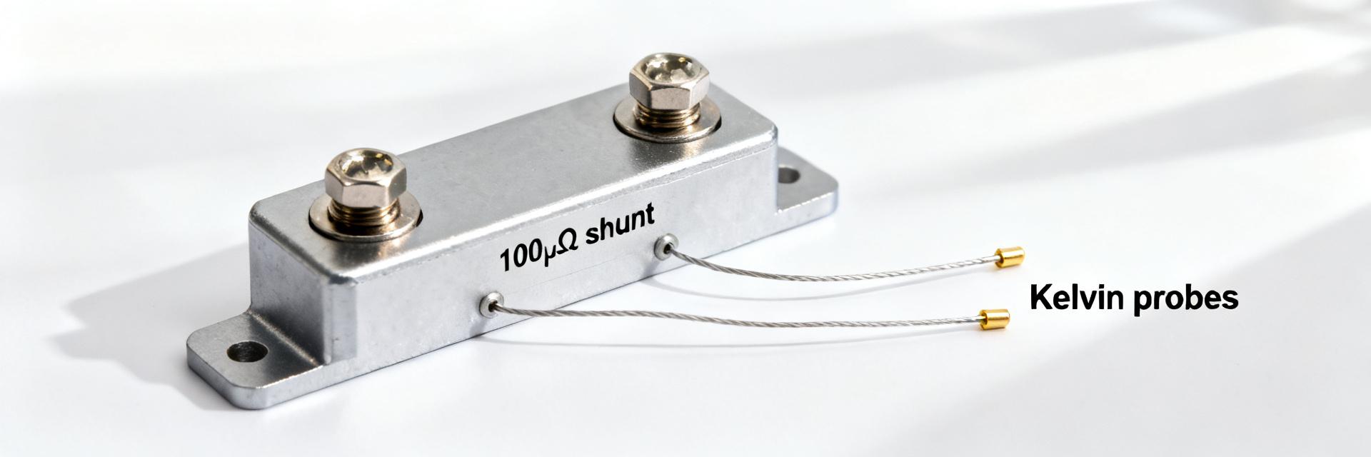
100µΩ Shunt Resistor Report: Precision Specs & Test Data
Demand for sub‑milliohm current sensing has risen sharply in high‑power battery systems and power conversion equipment; designs increasingly require 100µΩ shunt resistor measurements with millivolt‑le…
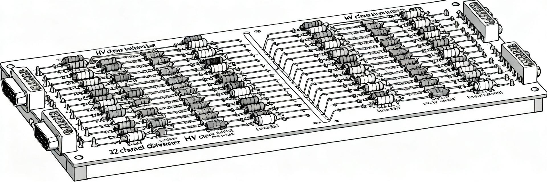
AD45336KSTZ: Latest Performance Report & Key Specs
Latest datasheet figures and bench verifications show the AD45336KSTZ delivers tightly matched 32-channel divider performance with stable operation across standard industrial temperature ranges. This …
STGWA30IH160DF2: Power & Key Electrical Specs Report
2026-06-27 10:15:24
NXH600N105L7F5S1HG performance report: Specs & Metrics
2026-06-26 10:16:24
NXH600N105H7F5S1HG: Thermal & Efficiency Report for IGBT
2026-06-24 15:59:18
ULH 500W Metal-Clad Resistor Performance Report & Specs
2026-06-23 10:15:19
ULV 500 resistor: Performance Data & Key Specs Explained
2026-06-21 10:18:17
Read more