


Helping you save cost and time.

Provide reliable packaging for your goods.

Quick and reliable delivery to save time.

Excellent after-sales service.
New Product Launch
More +


Hot Selling Parts


Blog
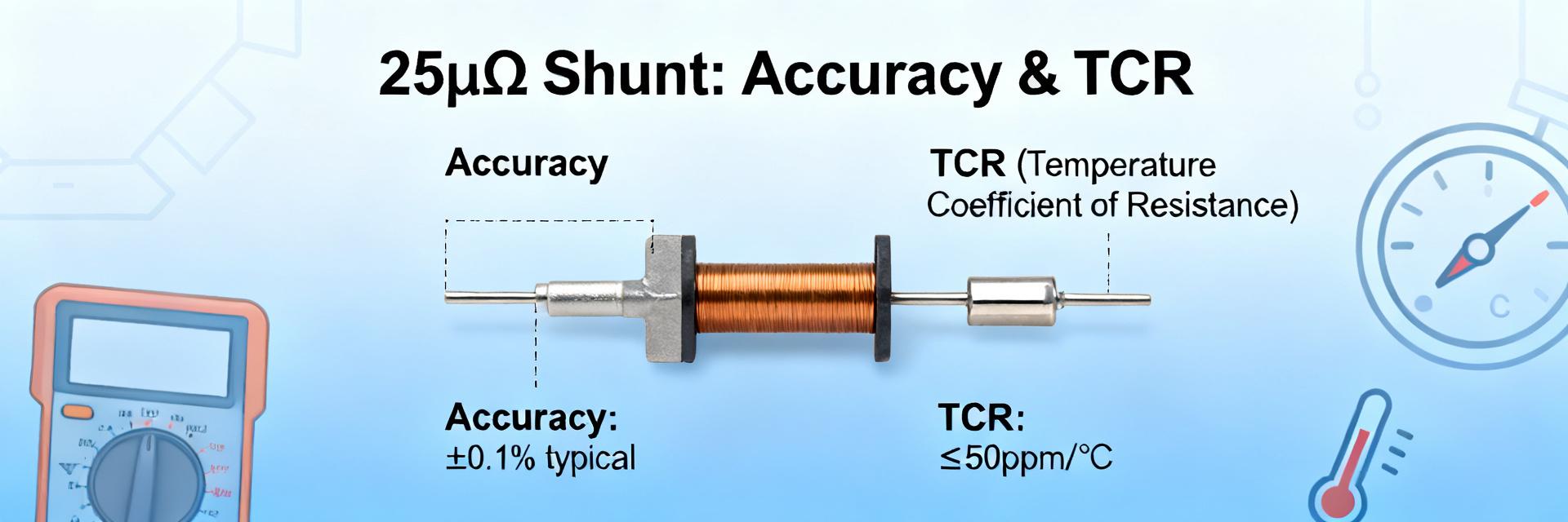
HoFL3-8536 25µΩ 0.5% Shunt Resistor: Measured Specs
Bench measurements of the HoFL3-8536-25uR-0.5% characterized DC accuracy, temperature behavior, and noise performance to judge suitability for precision current sensing. Tests covered currents from 0.…

HoFL3-8436-B shunt datasheet: key specs & test data
A 25 µΩ shunt resistor produces 2.5 mV at 100 A and dissipates 0.25 W; at 500 A it produces 12.5 mV and dissipates 6.25 W — numbers that define thermal, accuracy and mounting choices. This guide break…
HoFL3-8536 50 µΩ Shunt: Measured Specs & Field Data
2026-07-12 10:39:17
HoFL3-6918 50µΩ Shunt Datasheet: Precise Specs & Limits
2026-07-11 10:14:18
250µΩ shunt resistor HoFL3-8518-B: Complete Datasheet
2026-07-10 10:04:17
100 µΩ 50W Shunt Resistor: Precision Data & Bench Tests
2026-07-09 10:14:20
HoFL3-6918 100µΩ Datasheet: Quick Electrical Specs
2026-07-08 11:06:19
Read more