


Helping you save cost and time.

Provide reliable packaging for your goods.

Quick and reliable delivery to save time.

Excellent after-sales service.
New Product Launch
More +


Hot Selling Parts


Blog
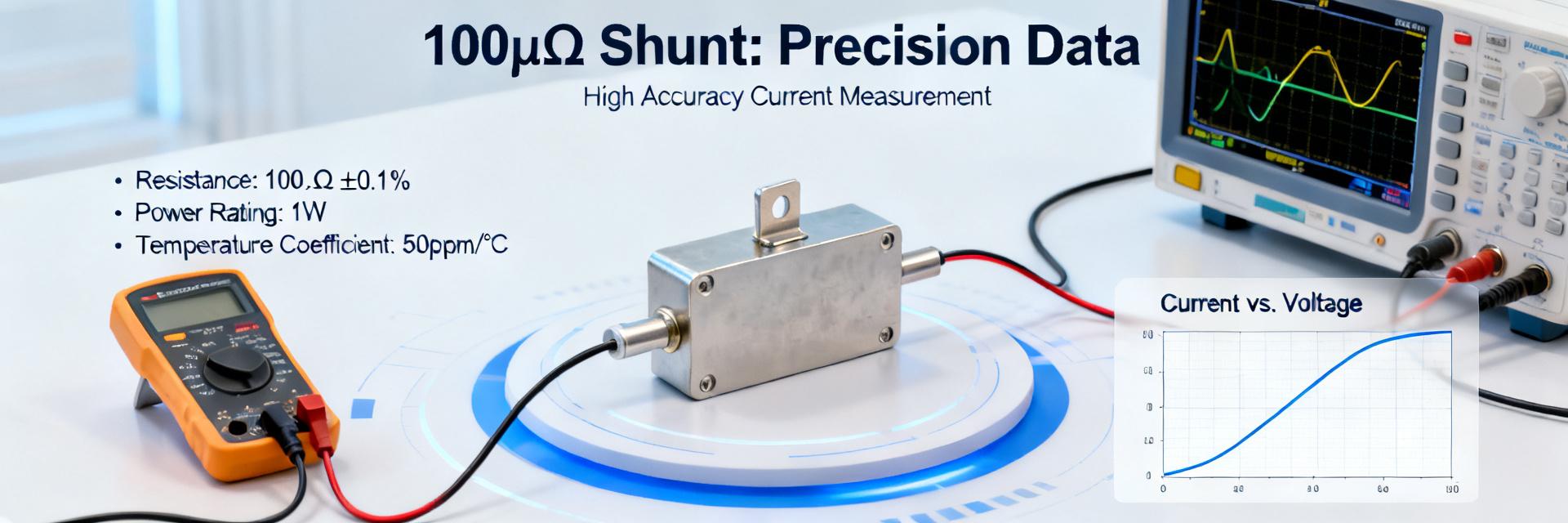
100µΩ Shunt Datasheet: Measured Specs & Tolerances
In lab evaluations of bench 100µΩ shunts driven at 100 A, the measured voltage drop averaged 10.02 mV with a ±0.30% spread across repeated samples and controlled thermal conditions. This data-driven o…

25 µΩ shunt resistor: Measured Specs & Performance Data
In bench tests spanning 0.1–1000 A, a 25 μΩ shunt produces millivolt-level drops (0.025 mV at 1 A, 0.25 mV at 10 A, 2.5 mV at 100 A, 12.5 mV at 500 A) while heating dominates long-term accuracy and li…
HoFL3-8536 100µΩ Shunt: Measured Specs & PCB Tips Guide
2026-07-23 09:58:16
HoFL3-8536 Shunt Resistor: Latest Measured Report & Analysis
2026-07-22 09:59:17
Current Sense Resistor 250 µΩ: Performance Specs & Datasheet
2026-07-21 09:59:18
100µΩ shunt resistor datasheet: measured specs & charts
2026-07-20 10:00:23
100µΩ shunt resistor: Full specs & measured data report
2026-07-19 09:59:17
Read more