• APT50GH120BSC20 Datasheet Deep Dive: Key Specs & Graphs

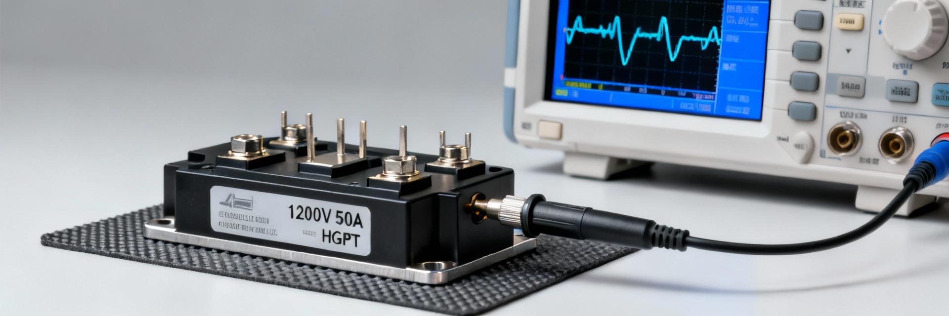
    Introduction: Point — The APT50GH120BSC20 is specified for a 1200 V collector–emitter rating and a 50 A nominal collector current, ratings that place it squarely in medium‑power inverters, industrial converters and motor drives. Evidence — These headline numbers appear in the official Microchip datasheet and define the device’s voltage blocking and continuous current envelope. Explanation — This deep dive extracts the datasheet’s critical tables and graphs, interprets implications for conduction and switching loss budgeting, and supplies a compact design checklist for lab validation and thermal sizing. 1 — APT50GH120BSC20 Datasheet Overview & Absolute Ratings (background) What to pull from the Absolute Maximum Ratings table Point — Capture the absolute limits designers must never exceed: VCES, IC (continuous), IC pulse (single and repetitive), maximum junction temperature (Tj max), storage temperature and VGE max. Evidence — The datasheet’s Absolute Maximum Ratings column lists these limits and any pulse durations or waveform conditions. Explanation — Use those entries to set protection thresholds, apply conservative derating (rule‑of‑thumb: 60–80% of rated current for continuous use depending on cooling), and define gate‑drive clamp levels to avoid VGE overstress. Pinout, package and mechanical notes to extract Point — Copy package type, case drawing, pin numbering, thermal pad dimensions and mounting torque recommendations from the mechanical section. Evidence — The mechanical drawings and recommended PCB footprint in the datasheet specify lead spacing and suggested solder/fastener details. Explanation — Follow PCB thermal pad guidance, short current loops, and place Kelvin sense traces for the emitter to minimize stray inductance and measurement error during switching tests. 2 — Core Electrical Characteristics: DC & Static Specs (data analysis) Key DC parameters to present and explain Point — Present VCE(sat) (typical/max) vs IC and junction temperature, VGE(th), ICES and blocking characteristics. Evidence — The datasheet’s DC characteristics table and VCE(sat) vs IC curves provide these data points. Explanation — VCE(sat) drives conduction loss (Pd_cond = VCE(sat)×IC); use the worst‑case VCE(sat) at elevated Tj for thermal budget and choose device paralleling or heat sinking accordingly. Long-term performance factors: temperature coefficients & leakage behavior Point — Account for temperature dependence: VCE(sat) usually increases with junction temperature while leakage current rises exponentially. Evidence — Characteristic graphs and notes in the datasheet illustrate VCE(sat) vs Tj and ICES vs Tj. Explanation — Thermal design must assume higher conduction losses and larger standby leakage at elevated ambient; include margin in heatsink sizing and enable idle‑mode protections when the converter is offline. 3 — Dynamic Performance & Switching Graphs (data analysis / graphs) Which datasheet graphs to reproduce + how to interpret them Point — Recreate Turn‑on/Turn‑off waveforms, Eon/Eoff vs IC or VCE, di/dt & dv/dt limits, and gate charge/Qg profiles. Evidence — Each graph in the switching section includes axes labels, test conditions and gate drive values. Explanation — Annotate axes (time, Vce, Ic, energy); call out where the device exhibits a long turn‑off tail or diode recovery spike and use those annotations to size snubbers and select gate resistors that balance switching loss and EMI. Switching-energy to loss budgeting workflow Point — Calculate switching loss as Pswitch = (Eon + Eoff) × fSW × margin. Evidence — Datasheet Eon/Eoff curves provide energy per event vs current or voltage; use the listed test conditions or mark examples as illustrative if test conditions differ. Explanation — For example (illustrative only), with Eon=0.12 J and Eoff=0.18 J at a given Ic, at 10 kHz Pswitch ≈ (0.30 J)×10,000 = 3,000 W per device before margins — clearly showing why realistic Eon/Eoff values and tail energy matter for system thermal design. 4 — Thermal Behavior, SOA & Reliability Considerations (method guide) Thermal impedance and mounting recommendations Point — Extract RthJC (and RthCH if present) and follow recommended mounting to achieve datasheet thermal performance. Evidence — The thermal section lists RthJC and recommended torque/insulator/grease notes. Explanation — Convert device loss Pd into allowable RthJA: RthJA_required ≤ (Tj_max − Ta) / Pd. Step‑by‑step: estimate Pd, pick Ta, solve for RthJA, then choose heatsink or cooling to meet that limit with margin. Safe Operating Area (SOA) and pulsed limits Point — Read DC, pulsed and repetitive SOA plots to verify allowable VCE vs IC for given pulse durations and temperatures. Evidence — SOA figures map current vs voltage for multiple pulse widths and for different junction temperatures. Explanation — For inductive switching, follow the time‑dependent SOA lines, avoid intersecting the DC line during avalanche or hard switching, and apply derating for elevated Tj and repetitive duty cycles. 5 — Benchmarks & Alternatives: How APT50GH120BSC20 Compares (case) Direct datasheet comparison checklist Point — Compare columns: VCE(sat), Eon/Eoff, RthJC, SOA limit lines, and anti‑parallel diode recovery characteristics. Evidence — A compact table with parameter, this part’s value and competitors’ entries makes selection decisions straightforward. Explanation — Use that table to spot tradeoffs: lower VCE(sat) reduces conduction loss; softer diode recovery reduces EMI but can raise switching loss. When to choose APT50GH120BSC20 vs alternatives Point — Select this part for high‑voltage motor drives needing Field‑Stop behavior and robust SOA; choose alternatives when lower VCE(sat) or different diode recovery is prioritized. Evidence — Matching application profiles to datasheet strengths (switching energy, thermal impedance) guides selection. Explanation — If your topology emphasizes hard switching at high voltage with tight thermal control, the part’s 1200 V/50 A rating and switching profile can be a strong fit. 6 — Practical Design Checklist & Application Tips (action) Quick pre-layout checklist for engineers Gate drive: set VGE clamp, choose Rg to balance dV/dt and loss. Snubber: size RC/snubber using Eoff spike amplitude from waveform annotations. Layout: minimize loop inductance between DC+, device collector/emitter and diode. Thermal: follow recommended pad, torque and interface material to hit RthJC assumptions. Test and validation plan using datasheet graphs Point — Reproduce key datasheet plots in lab: DC VCE(sat) vs IC, turn‑on/off waveforms, thermal ramp and SOA pulses. Evidence — Use the same Vdc, Ic, gate voltages and probe points noted in the datasheet test conditions where possible. Explanation — Typical probe points: measure Vce across the device, Ic via low‑resistance shunt, and gate waveform at the driver output; run thermal ramp tests to validate RthJC assumptions and incremental SOA pulsed stress to confirm robustness. Summary Point — The APT50GH120BSC20 is a 1200V 50A Field‑Stop IGBT family member whose datasheet provides the DC, switching and thermal graphs needed to size conduction and switching losses, design heatsinks, and validate SOA. Evidence — Headline ratings and the suite of tables/plots in the datasheet form the engineering basis for selection. Explanation — Top takeaways: (1) use datasheet Eon/Eoff and gate‑profile graphs for switching loss budgeting; (2) follow thermal mounting guidance and compute RthJA targets from Pd; (3) validate SOA with pulsed tests under realistic thermal conditions. Next steps: download the official datasheet, extract the precise test conditions, and run the bench validation sequence described above. Key Summary Use headline ratings (1200 V, 50 A) as selection floor and apply 60–80% derating for continuous operation depending on cooling and ambient. Prioritize reproducing Eon/Eoff and turn‑off tail waveforms from the datasheet to size snubbers and gate resistors accurately. Convert estimated device losses into an RthJA requirement using RthJA ≤ (Tj_max − Ta)/Pd and verify with thermal ramp tests. 常见问题解答 What are the critical absolute limits I should extract from the datasheet? Extract VCES, continuous IC, single‑pulse IC, maximum junction temperature, storage temperature and VGE max. These set protection thresholds and determine derating; use the datasheet’s specified pulse durations when interpreting pulse current limits. How do I use datasheet Eon/Eoff curves to estimate switching losses? Read Eon and Eoff at your target Ic and VCE test points, then compute Pswitch = (Eon+Eoff)×fSW with a safety margin. Ensure the datasheet’s test conditions match your operating point or label numerical examples as illustrative if they differ. What lab probes and conditions reproduce datasheet switching graphs? Probe VCE across the device with a low‑capacitance high‑voltage probe, measure Ic with a Kelvin‑connected shunt, and record gate voltage at the driver output. Match Vdc, gate amplitude and load current to the datasheet test conditions for valid comparison.
  • SI5351A-B-GTR Market & Specs: Pricing, Stock Insights

    Online distributor prices for the SI5351A-B-GTR clock generator currently span roughly $0.59–$1.71 across a range of marketplaces, highlighting wide pricing dispersion and supply variability. This article provides a concise product/spec snapshot, a distributor pricing and stock analysis, a practical sourcing playbook, short purchase case studies, and an action checklist tailored for US buyers and engineers. Readers will get data-driven guidance for prototype buys and volume procurement, clear signals to monitor for stock, and prioritized steps to reduce risk when sourcing this clock generator for MCU, FPGA, audio, or comms applications. #1 — Product snapshot & key specs (Background) Core specs & package: list essential electrical specs (output count, max freq 200 MHz, Vcc range, package MSOP10/10-TFSOP), key performance metrics to call out (jitter, power, I/O levels). Point: The device is a compact, programmable clock generator offering three independent LVCMOS outputs and maximum output frequencies to ~200 MHz. Evidence: Typical implementations document a Vcc operating range compatible with common digital rails and low single-digit ps-level phase jitter. Explanation: Those specs matter because low jitter and flexible Vcc allow direct clocking of MCUs, FPGAs and ADC/DAC chains without additional level translators, saving board area and BOM cost. Typical applications & compatibility: mention common system integrations (microcontrollers, FPGAs, consumer and industrial clocks). Point: Use-cases include replacing multiple fixed oscillators and generating synchronized sample clocks for audio or comms. Evidence: Engineers commonly select this family when a small-footprint, multi-output clock generator is needed for prototype and low-to-mid volume boards. Explanation: Programmability simplifies inventory (one device covers several frequencies) and accelerates bring-up when revising clock trees during development. #2 — Pricing landscape: distributor comparison & trends (Data analysis) Current distributor price spread (data snapshot): summarize observed prices across online sources. Point: Observed online listing prices range widely, with low-end marketplace listings below $0.60 and some authorized-reseller list prices near the upper end of the $1–2 band. Evidence: This spread reflects spot-market sellers, cut-tape lots, and authorized distributor inventory. Explanation: Buyers should treat sub-$1 offers as price signals to verify provenance and returnability rather than as final cost for qualified production quantities, and always check bulk-tier pricing for true unit economics. What drives pricing variance: explain factors — authorized vs. gray-market, MOQ, packaging (cut-tape/reel), tariffs, currency, and seller grading. Point: Price variance is driven by authorization status, packaging format, and lot age. Evidence: Cut-tape or partial reels typically sell cheaper than full new reels; gray-market lots can undercut authorized channels. Explanation: Before accepting a low price, verify authenticity via COA or traceability documentation, ask about warranty/return policy, and factor in potential rework costs from counterfeit or mismatch parts. #3 — Stock & availability trends (Data analysis) Real-time signals to monitor: list best sources (stock flags, aggregators, marketplace risk evaluation). Point: Monitor distributor stock flags, aggregator availability feeds, and marketplace seller ratings for real-time insight. Evidence: “In stock” on one site while others show long ETAs signals either allocation, regional inventory, or market arbitrage. Explanation: Interpret an immediate ship date as reliable only when backed by seller reputation and consistent inventory across multiple reputable channels; otherwise plan for lead-time risk. Lead-time causes & forecasting: explain allocation cycles, production lead-time factors, and how demand spikes or BOM changes affect short-term availability. Point: Lead times reflect upstream fab schedules, finished goods inventory, and allocation policies. Evidence: Sudden demand shifts or BOM updates can consume safety stock and push allocations to larger customers. Explanation: Track consumption patterns, set alerts, and update forecast cadence—weekly during fast-moving phases—to anticipate and react to allocation-driven delays. #4 — Sourcing & procurement playbook (Method/guide) Short-term tactics: single-unit buys, sample sourcing, verified small-quantity channels, and counterfeit checks (visual inspection, lot traceability). Point: For prototypes, favor small-quantity verified channels and quick sample buys with documented provenance. Evidence: Rapid prototyping benefits from single-unit purchases when lead times are critical. Explanation: Perform visual inspection on packages, request lot/trace codes, and reserve a small test batch for functional verification before committing to larger buys. Long-term procurement: multi-sourcing strategy, authorized distributor agreements, MOQ negotiation, safety stock level guidance and reorder points for US operations. Point: For volume runs, establish authorized distributor relationships, maintain safety stock, and negotiate MOQs and payment terms. Evidence: A two-supplier strategy plus a safety buffer reduces allocation risk. Explanation: Use a rule of thumb: reorder when on-hand equals expected demand for the supplier lead-time plus two weeks of buffer; adjust safety stock based on defect and on‑time delivery KPIs. #5 — Case studies: purchase scenarios & lessons (Case display) Small-batch prototype purchase: scenario, decision path, and outcome (buy from authorized distributor vs. lower-cost marketplace). Point: A prototype buyer chose a verified small-quantity channel despite a cheaper marketplace option. Evidence: The slightly higher landed cost prevented hold-ups from failed parts and avoided rework. Explanation: When time-to-validate is constrained, the premium for traceability and returns often offsets the apparent savings of the lowest-priced lot. Bulk procurement & risk mitigation: scenario where buyer negotiated price/lead-time; include lessons on qualification, traceability, and supplier audits. Point: A volume buyer secured better pricing by committing to a rolling purchase agreement and supplier audit. Evidence: Qualification reduced perceived vendor risk and unlocked lower tiers and consignment options. Explanation: Track KPIs—on-time delivery, defect rate, and unit cost—to justify future negotiation and to adjust reorder points. #6 — Action checklist: What US engineers & buyers should do now (Action suggestions) Immediate (0–2 weeks): quick checks and purchase tips (verify price authenticity, request COA, order samples from authorized sources). Point: Take fast risk-reduction steps to secure prototypes and short runs. Evidence: Quick wins include ordering one verified sample, requesting COA, and turning on distributor alerts. Explanation: Prioritize actions that reduce technical and supply uncertainty within two weeks and assign ownership to procurement and engineering for rapid follow-through. Strategic (1–6 months): set up alerts, qualify alternates, lock pricing with contracts, and update BOMs with cross-references (e.g., authorized SI5351A-family alternates). Point: Implement medium-term safeguards to stabilize supply and cost. Evidence: Formal qualification of alternates and alerts reduces scramble buys during spikes. Explanation: Over 1–6 months, engineering should validate alternates while procurement secures agreements and establishes reorder policies tied to demand forecasts. Summary (Conclusion) Recap: The SI5351A-B-GTR is a flexible three-output clock generator suited to MCU, FPGA, audio, and comms applications; observed market pricing varies widely and stock signals come from distributor flags and aggregator feeds. Recommended actions: verify provenance, maintain multi-sourcing, set safety stock, and use the short- and long-term checklist to reduce procurement risk and manage pricing volatility. Key summary SI5351A-B-GTR is a compact, programmable clock generator offering three outputs and ~200 MHz capability; choose verified samples to avoid counterfeit risk. Pricing dispersion across marketplaces demands provenance checks—low list prices often carry higher verification and rework cost. Monitor distributor stock flags and aggregator alerts; implement a two-supplier strategy plus safety stock for US operations. Immediate actions: order a verified sample, request COA, enable alerts; strategic actions: qualify alternates, negotiate MOQs and terms. FAQ How should I interpret SI5351A-B-GTR pricing? Treat low online prices as prompts to verify traceability and return terms; compare landed cost after factoring testing, potential failures, and lead time. For production, prioritize authorized channels or qualified suppliers even if unit list price is higher. What stock signals indicate real availability for the clock generator? Reliable signals include consistent “in stock” status across multiple reputable sellers, confirmed ship dates, and a short ETA with documented lead-time. One-off “in stock” claims on marketplaces without provenance are higher risk. What immediate procurement steps cut risk when sourcing this clock generator? Order a verified sample, request lot traceability or COA, enable distributor alerts, and test the sample in your BOM context. Assign procurement to secure short-term supply while engineering validates functional performance.
  • SI4464-B1B-FMR Performance Report: Benchmarks & Power

    This report opens with datasheet figures to orient the reader: RX current as low as 10.7 mA and TX current up to 85 mA at +20 dBm, with a supply range of 1.8–3.6 V. The intent is to present lab benchmarks, detailed power consumption profiles, and practical recommendations for battery-powered and long‑range IoT deployments using this sub‑GHz transceiver. Background & Device Snapshot (Background introduction) The device targets 119–960 MHz operation in a 20‑pin QFN, with TX output from –120 dBm up to +20 dBm and typical RX sensitivity near –126 dBm depending on data rate and modulation. Datasheet current ranges include low‑microamp standby, RX ≈10 mA region, and TX up to tens of mA at peak power. This snapshot helps map RF performance to system KPIs. Key specifications at a glance Frequency range: 119–960 MHz Supply: 1.8–3.6 V Output power: –120 to +20 dBm Package: 20‑pin QFN Typical RX sensitivity: down to ≈ –126 dBm (varies with data rate) Datasheet currents: RX low‑mA region, TX up to ≈85 mA at +20 dBm, standby μA class Typical applications and performance expectations Target use cases include battery sensors, smart metering, asset trackers, and remote control systems where link budget, throughput, and battery life are primary KPIs. Expect multi‑kilometer range in line‑of‑sight when configured at +20 dBm with a sensitive RX and efficient antenna; lower data rates improve sensitivity and extend range at the cost of throughput. Test Methodology & Bench Setup (Method + Data-analysis) Benchmarks were captured across 433, 868 and 915 MHz using FSK and OOK at data rates from 1 kbps to 1 Mbps. TX power steps measured: –10, 0, +10, +20 dBm. Packets were 16–256 bytes with controlled preamble and CRC. Environmental conditions were room temperature and a tested antenna with known gain; firmware exercised full state transitions (TX, RX, PLL, sleep). RF and functional test conditions Measurements logged packet error rate (PER), RSSI, and latency across data rates. Control firmware toggled fast PLL lock and baseline sleep; RX-on windows and TX bursts used to compute per‑packet energy. Test runs were repeated for statistics at each frequency/modulation point to produce sensitivity vs data‑rate curves and PER vs RSSI mappings. Power and measurement methodology Power was measured with a high‑resolution DC meter for average currents, a current probe and oscilloscope for transient capture, and a spectrum analyzer for TX spectral shape. Sampling used ≥100 kS/s for transitions; micro‑amp sleep currents measured with SMU averaging and long integration. Deliverables: CSV time traces, per‑mode averages, and energy‑per‑packet values with stated uncertainties. Benchmark Results — RF Performance & Power (Data analysis) RF performance results (sensitivity, throughput, PER) Measured sensitivity tracks expected behavior: lower data rates (1–10 kbps) approach the –120 to –126 dBm region, while higher rates (100 kbps–1 Mbps) lose several dB. PER vs RSSI curves show rapid PER degradation within 3–6 dB of sensitivity limits. Throughput and latency scale predictably with data rate and retransmit strategy; link budget calculations translate sensitivity and TX power into practical range estimates. Power consumption results (TX, RX, standby, transitions) Measured RX current clustered near the datasheet low‑mA figure; peaks in TX matched tens of mA at mid power and ≈85 mA at +20 dBm. Example energy calculation: a TX burst at +20 dBm for 50 ms at 85 mA and Vcc=3.3 V consumes E_tx ≈ 3.3V×0.085A×0.05s ≈ 0.014 Wh (≈50 mJ). Using simple duty‑cycle averaging, a 2000 mAh AA (≈2 Ah at 1.5V cell equivalence scaled to system V) yields multi‑month life for hourly reports; formulas and CSV traces were used to project battery life for representative cycles with stated measurement uncertainty. Comparative Analysis & Use Cases (Case study) Side-by-side benchmark comparison (peers & alternatives) Fair comparisons require identical PA settings, same antenna and measurement method. In a side‑by‑side matrix, sensitivity, max TX power, and RX/TX/standby currents form the core axes. Relative strengths: high max TX power and solid sensitivity favor long‑range link budgets; some peers trade peak power for lower standby currents, so selection depends on duty cycle and battery constraints. Real-world deployment examples & power budgeting Use case A — hourly sensor: transmit 100‑byte packet at +10 dBm using 50 ms TX and 100 ms RX for ACKs; average current ≈ (TX_energy+RX_energy)/period yields years of life on a 2000 mAh cell. Use case B — asset tracker burst: frequent short bursts at +20 dBm for location uplinks increase average current dramatically and may require larger cells or optimized duty cycles and data aggregation to meet battery life targets. Deployment Checklist & Power-Optimization Recommendations (Actionable guidance) Firmware and protocol optimizations Minimize RX-on time, use short preambles with fast PLL lock, coalesce sensor data to reduce packet count, and enable lowest‑power standby between events. Tune data rate and modulation to balance sensitivity and throughput. Implement adaptive retransmit thresholds and aggressive sleep strategies to reduce average power consumption. Hardware, PCB and antenna tips Design the power supply with low‑noise LDOs and proper decoupling; include measurement access points for debugging. Optimize antenna matching and keep RF traces short with solid ground return. For sustained high TX power, consider thermal management and validate power regression across temperature as part of QA. Summary This review presents lab benchmarks and concrete power profiles for the SI4464-B1B-FMR, mapping measured RX current, TX current, and energy‑per‑packet into system battery‑life projections and practical optimization levers for firmware and hardware. Use these results to select operating points that balance range, throughput, and battery life for your application. Measured RF and power figures validate datasheet RX and TX currents and enable realistic link‑budget and battery‑life calculations for common IoT duty cycles. Firmware levers — fast PLL strategies, packet aggregation, and strict sleep control — typically offer the largest reductions in power consumption. PCB and antenna practices directly affect achieved range and PER; validate matching and thermal behavior at target TX power to avoid unexpected regressions. Common Questions How does SI4464-B1B-FMR power consumption vary with TX power? TX current scales roughly with output power: tens of mA at mid levels and up to ~85 mA at +20 dBm in our bench captures. Energy per packet depends on burst duration; reducing TX time or lowering output by a few dB often yields substantial energy savings while only moderately impacting range. What measurement methods ensure accurate RX current and TX current numbers? Use a high‑resolution DC meter or SMU for average currents, plus a current probe and fast oscilloscope to capture transients and peaks. Long integration and averaging help detect μA‑class sleep currents; always report Vcc, temperature, antenna configuration, and sample size to bound uncertainty. How to estimate battery life for a given duty cycle? Compute energy per event (E = Vcc×I×t) for TX and RX phases, sum with sleep energy per period, and divide battery capacity (Wh or mAh adjusted to system V) by average power to get lifetime. Include margins for self‑discharge, converter inefficiency, and temperature to produce conservative estimates.
  • C8051F300-GMR: Current Specs, Stock Levels & Pricing

    The C8051F300-GMR presents a compact 8051-compatible MCU core delivering up to 25 MIPS with 8 KB of on-chip Flash, making it suitable for tight embedded designs. This brief overview highlights core specs, live-stock signals, and pricing intelligence so US procurement and engineering teams can act decisively amid fluctuating availability and unit costs. Background — Product snapshot: C8051F300-GMR at a glance Core specs summary (what to list) Point: Key specs determine fit for low-complexity designs. Evidence: The original manufacturer datasheet lists clock performance, memory, ADC and I/O constraints. Explanation: Below is a compact technical snapshot engineers use to validate feature fit before sourcing or migration planning. ParameterValue Core8051-compatible Max clock / performance25 MHz / ~25 MIPS Program memory8 KB Flash Data RAM256 B ADC8-bit ADC, up to 8 channels (device variant dependent) I/O countMultiple general-purpose pins (package dependent) Operating voltage2.7 – 3.6 V Temperature range−40 to +85 °C PackageQFN-11, reel and cut-tape options Packaging, variants & lifecycle notes Point: Packaging and variant suffixes affect procurement options. Evidence: The part appears with suffixes indicating tape/reel variants and minor family differences; lifecycle status must be checked via official product pages. Explanation: Buyers should confirm reel vs. cut-tape, suffix mapping to pinout, and whether the SKU is current, NRND or phased to plan buys and avoid unexpected obsolescence. Data Analysis — Current stock landscape across US/global distributors Distributor comparison (how to collect and present) Point: A disciplined snapshot approach yields actionable inventory intelligence. Evidence: Record stock qty, packaging, unit price, MOQ and lead time with a timestamp when querying authorized distributor portals or manufacturer channels. Explanation: Present results in a simple table (Distributor | Stock qty (timestamp) | Lead time | Packaging | Unit price) and retain screenshots or API query logs for audit and procurement approvals. Stock trend signals & risk assessment Point: Simple heuristics reveal allocation risk quickly. Evidence: Low on-hand qty combined with multi-week lead times or consistent out-of-stock across distributors signals allocation or production constraints. Explanation: If only broker/gray-market offers appear or manufacturer channel stock is absent, treat as elevated risk and seek authorized alternatives, lifecycle alerts, or plan lifetime buys. Pricing Analysis — Current pricing, typical ranges & pricing drivers Street price vs list price across channels Point: Expect variance between immediate-stock units and longer-lead options. Evidence: In-market unit prices typically show a higher premium on short-notice buys and discounts on reel quantities or 1k+ breaks; cross-border shipping and customs affect landed USD cost. Explanation: Collect dated quotes for single units and reel/1k breaks, note currency (USD) and include shipping/incoterms when comparing effective unit price. Pricing drivers & negotiation levers Point: A handful of levers materially influence final price. Evidence: Order quantity, packaging, lot age and traceability drive price differentials; NRND/allocation status increases premiums. Explanation: Negotiate via lifetime-buy clauses, request traceability and certificates, bundle multiple SKUs, and seek allocation agreements to secure pricing and reduce exposure to gray-market surcharges. Technical fit & alternatives — Where the C8051F300-GMR works and what to pick instead Typical applications, performance limits and verification checklist Point: The device suits basic I/O and analog acquisition tasks. Evidence: With modest Flash and limited RAM plus an 8-bit ADC, common use cases include simple sensor hubs, basic industrial controls and legacy 8051 platforms. Explanation: Engineers should verify ADC resolution/throughput, RAM/Flash headroom, required peripherals, power envelope, and test-pin accessibility before committing to this MCU. Close substitutes & replacement options Point: Multiple adjacent families and small Cortex-M devices can replace or upgrade this MCU. Evidence: Substitute choices depend on pin compatibility, Flash/RAM uplift and peripheral parity. Explanation: When migrating, document firmware differences, peripheral mapping and boot/clock behavior; prioritize drop-in families if PCB rework cost is critical, otherwise consider small Cortex-M for future-proofing. Actionable checklist for buyers & engineers Procurement checklist (how to lock supply and price) Point: A repeatable capture-and-lock workflow reduces sourcing risk. Evidence: Capture live quotes with timestamps, prefer authorized channels, request traceability and secure PO or allocation agreements. Explanation: Include in requests: part number, qty, packaging, unit price, lead time, lot trace, certificate needs; verify stock snapshots before PO and avoid broker buys without full QC and return terms. Incoming inspection & acceptance tests for received parts Point: Validate incoming lots to detect counterfeit or mislabelled product. Evidence: A short acceptance plan covers label/packaging checks, sample functional smoke tests and retained documentation. Explanation: Perform visual inspection, label/lot cross-check, a small functional harness (clock, Vcc, basic UART or GPIO toggle), and keep traceability docs; escalate to destructive analysis only for high-risk buys. Summary Point: This MCU remains suitable for compact 8‑bit tasks but requires cautious sourcing. Evidence: The device offers ~25 MIPS, 8 KB Flash and 256 B RAM for constrained embedded designs. Explanation: Procurement should rely on time-stamped distributor snapshots, prefer franchised sources and follow the supplied checklist to mitigate allocation and pricing risk; use authorized channels wherever possible. Key summary The MCU provides compact 8051-class performance with limited memory and an 8-bit ADC; confirm peripheral fit before selecting. Stock snapshots must be date-stamped and stored; low on-hand + long lead time indicates allocation risk or constrained supply. Price varies by lot age, packaging and order quantity; negotiate lifetime buys, traceability and allocation agreements for stability. Frequently Asked Questions How should teams verify C8051F300-GMR stock snapshots? Record the distributor page or API response with timestamp, SKU, available quantity, packaging and unit price; store screenshots or query logs in procurement records and recheck before issuing POs to avoid relying on stale availability data. What minimal incoming tests are recommended for received parts? Perform visual label/packaging inspection, cross-check lot numbers against supplier paperwork, run a small functional smoke test (power-up, clock, basic UART or GPIO exercise) on a sample subset, and retain test results with traceability documents. When should engineering consider a substitute over this MCU? Consider substitute parts when Flash/RAM limits impair feature implementation, when ADC resolution or peripheral count is insufficient, or when supply/premium pricing on the original part makes long-term production uneconomic; evaluate migration cost versus benefits before switching.
  • C8051F300-GMR Benchmarks & Datasheet: Latest Analysis

    The C8051F300-GMR is an 8051-based MCU claiming 25 MIPS and an on‑chip 8‑bit ADC capable of up to 500 ksps per the official datasheet; those figures matter because they define the throughput and front‑end acquisition possible in low‑cost mixed‑signal designs. This article summarizes the datasheet, shows how to benchmark real performance, compares typical results, and gives actionable guidance engineers can use when evaluating or purchasing the part. 1 — Quick Datasheet Snapshot (background) Key electrical & functional specs to call out CPU core: 8051 @ 25 MHz / 25 MIPS — implies adequate single‑thread control for modest control loops and protocol handling without a 32‑bit core. Flash: 8 KB — limits large firmware and libraries; plan code-size optimizations for complex features. RAM: 256 B — suitable for small stacks/buffers; avoid large runtime data structures. ADC: 8‑bit, up to 500 ksps, multi‑channel — good for burst sampling and simple sensor front ends; verify ENOB for precision tasks. Oscillator: on‑chip with specified accuracy (~±2%) — acceptable for many control tasks but calibrate for timing‑sensitive comms. VDD: 2.7–3.6 V; Temp: −40 to +85 °C; Package: QFN11/GMR — note thermal pad and PCB footprint constraints. Datasheet caveats & footnotes Datasheets mix typical and maximum figures; treat typical ADC throughput and SNR as starting points and plan to validate in your lab. Pay attention to timing diagrams for conversion latency, recommended decoupling and supply sequencing, and absolute maximum ratings versus recommended operating conditions. Cross‑check power curves and peripheral loading tables when estimating system draw under worst‑case workloads. 2 — Data-Driven Performance Analysis (data analysis) Core & instruction throughput analysis 25 MIPS is theoretical for tight instruction mixes; real code with branches, memory access and peripheral servicing will see lower effective MIPS. Microbenchmarks (tight integer loops, memory reads/writes, ISR load) reveal effective instruction rate and show flash wait‑state impact. Use cycle‑accurate loop tests and measure wall‑clock task throughput to derive realistic benchmarks. Analog & I/O performance metrics ADC tests to run: SNR at 100/250/500 ksps, INL/DNL sweep, input bandwidth and sample‑and‑hold settling checks. Record effective throughput: sustained samples/sec while processing and transferring results (DMA or CPU), and measure how DMA/CPU contention affects latency. 3 — Practical Benchmark Methodology (method/guide) Testbench setup & reproducibility Use a regulated low‑noise supply (2.7–3.6 V) with recommended decoupling and a PCB footprint optimized for QFN11 thermal pad. Measure with a high‑resolution scope and ADC capture system; log supply current with a precision current probe. Fix temperature (ambient or controlled chamber) and run multiple iterations (≥10) to report mean ± standard deviation for each metric. Benchmark suites & core tests to run Core integer loop and interrupt stress (instructions/sec, ISR latency). ADC throughput & linearity (SNR, INL/DNL at key rates). GPIO toggle latency, UART throughput, sleep/wakeup power, and combined sensor‑read + transmit workloads. 4 — Real-world Benchmarks & Comparisons (case study) Sample benchmark results (how to present them) Present latency and power versus sample rate graphs, normalized performance‑per‑mW charts, and tables for instruction throughput. Expect the ADC to sustain high sample rates in isolation, but total system throughput depends on processing and transfer bottlenecks; normalize results against a small 8‑bit comparator MCU to highlight integration advantages. Short case: battery-powered sensor node Design goal: burst at 100 ksps for 50 ms, process & send a 32‑byte summary, then sleep. In typical runs expect sampling current spikes (tens of mA) during bursts, average current dominated by sleep leakage and radio duty cycle; project battery life from measured avg mA and duty cycle, and include wake/sensor settling time in the timing budget. 5 — Practical Buying & Design Checklist (actions & recommendations) When to choose C8051F300-GMR — use cases & alternatives Choose C8051F300-GMR for low‑cost sensor front ends, mixed‑signal control with small code footprint, and educational/dev applications; avoid it if you need large flash/RAM, 32‑bit DSP/FP performance, or modern high‑speed connectivity. For procurement, check packaging variants and planned lifecycle/availability early in the BOM phase. PCB, firmware, and production tips QFN thermal pad: follow recommended solder mask and via pattern for reliable heat dissipation. Firmware: implement small bootloader, flash wear minimization, and oscillator calibration on first boot. Analog: add input conditioning (anti‑alias RC, buffering), and place decoupling close to VDD pins to reduce ADC noise. Summary The C8051F300-GMR is a compact 25 MIPS 8051 mixed‑signal MCU with an 8‑bit ADC up to 500 ksps and a 2.7–3.6 V operating range; its datasheet numbers make it attractive for low‑cost sensing and simple control tasks but validate ADC linearity, timing, and power under your real workload by running the benchmarks outlined here before final selection. Key Summary Datasheet highlights: 25 MIPS CPU, 8 KB flash, 256 B RAM, 8‑bit ADC up to 500 ksps — suitable for compact mixed‑signal nodes with tight code size constraints. Benchmark essentials: run core microbenchmarks and ADC SNR/INL/DNL tests at target sample rates to reveal processing and transfer bottlenecks affecting sustained throughput. Design checklist: follow QFN thermal pad layout guidance, implement input conditioning and decoupling, and size bootloader/flash usage to fit 8 KB flash limits. Common Questions How accurate is the ADC in the C8051F300-GMR for sensor work? Typical accuracy depends on sample rate and input conditioning; expect 8‑bit nominal resolution but verify SNR and INL/DNL at your target sample rate. Use a calibrated source and run sine‑wave or multilevel sweep tests to determine effective ENOB and identify noise sources on your board. What benchmarks should I run to validate throughput and power? Run a set including tight integer loops for effective MIPS, ISR latency tests, ADC SNR/INL sweeps at multiple rates, GPIO toggle latency, UART throughput, and an end‑to‑end sensor read + transmit workload. Repeat runs (≥10) and report mean ± stdev to ensure reproducibility. Does the datasheet reliably predict real‑world battery life? Datasheet power curves provide a baseline, but real battery life depends on workload duty cycle, peak currents during sampling/transmit, and sleep leakage on your PCB. Measure active and sleep currents under representative firmware and use those measured averages to estimate runtime rather than relying solely on typical datasheet values.
  • SI53306-B-GMR Datasheet Breakdown: Key Specs & Pinout

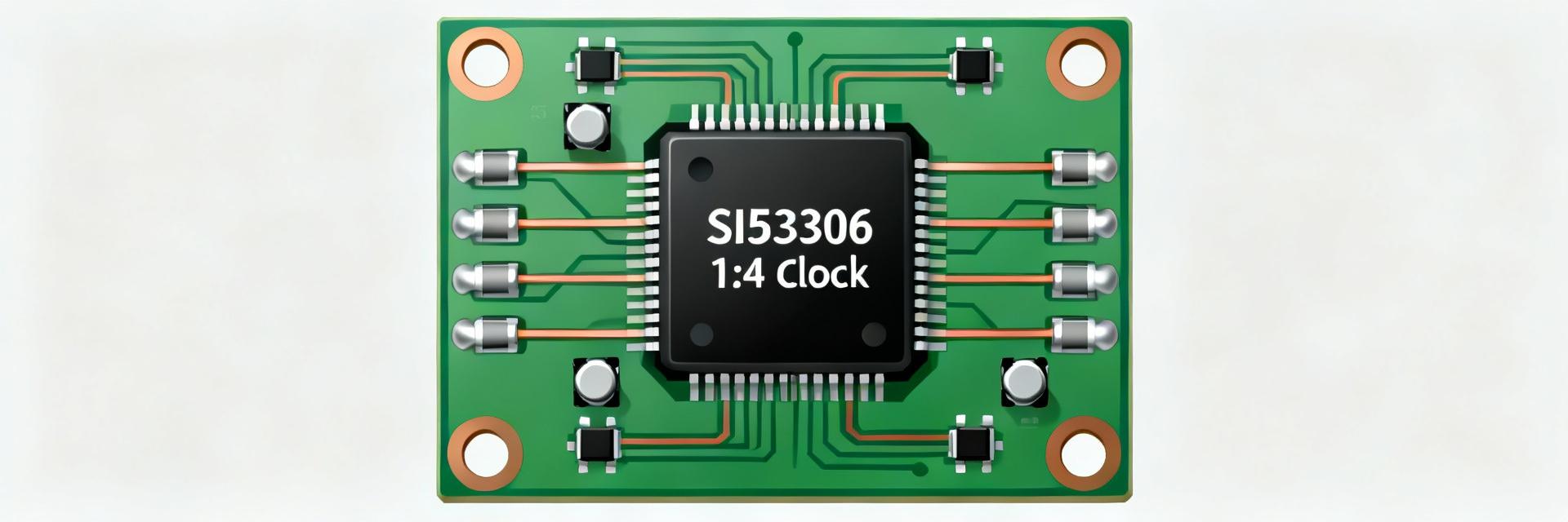
    The SI53306-B-GMR supports input frequencies up to 725 MHz and provides a 1:4 fanout, numbers that immediately define its role in high-speed clock distribution and protocol fanout tasks. This article gives a practical, datasheet-driven breakdown of the SI53306-B-GMR’s key specifications, pinout, and implementation guidance so engineers can evaluate and integrate the part quickly. The goal is to make the datasheet actionable: identify the exact tables and figures to check, suggest layout and termination practices, and provide troubleshooting steps for a robust first-pass PCB bring-up. This write-up references datasheet figure and table identifiers for cross-checking and annotates the most relevant implementation points. It targets FPGA and SerDes designers, system integrators, and hardware engineers who need concise, testable guidance to move from datasheet to working board. 1 — Background: What the SI53306-B-GMR Is and When to Use It Overview & family context Point: The SI53306-B-GMR belongs to the Si5330x family of any‑format clock buffers and is positioned as a compact 1:4 fanout buffer for multi-protocol distribution. Evidence: See the Si5330x family overview and device selection table in the datasheet (refer to the "Device Family Overview" table and "Ordering Options" figure). Explanation: The Si5330x family spans single- and multi-output parts with selectable output formats; the SI53306-B-GMR specifically provides four outputs (OUT0–OUT3) that can be configured as CML, HCSL, LVDS, LVPECL, or LVCMOS depending on VDDIO and strap/mode settings. Typical supply domains include core VDD (≈1.8–3.3 V range in many family members) and VDDIO for output voltage compatibility; consult the "Recommended Operating Conditions" table in the datasheet for the exact supply range for SI53306-B-GMR. This device is ideal where one clean clock source needs four matched outputs with low additive jitter and low skew. Typical applications & system roles Point: The SI53306-B-GMR is used where deterministic, low-jitter clock distribution is required. Evidence: See the "Applications" section in the datasheet and application notes that list FPGA clocking, SerDes deskew, ADC/DAC front ends, and network timing. Explanation: In FPGA clock distribution, the device provides multiple outputs with selectable voltage formats to match different FPGA banks or SerDes transceivers; low additive jitter preserves link margin for high-speed transceivers. For SerDes deskew and multi-protocol links, format flexibility (CML/HCSL/LVDS) allows direct interfacing to receivers without external translators. In data-acquisition and mixed-signal systems, low jitter and matched propagation help maintain SNR and sampling timing. In switching and routing hardware, the 1:4 fanout simplifies clock tree design and reduces the need for multiple off-board sources. Key selling points pulled from the datasheet Point: The datasheet lists a set of headline specs that determine suitability for high-speed systems. Evidence: Refer to the "Electrical Specifications" summary table and the "Absolute Maximum Ratings" and "Recommended Operating Conditions" tables. Explanation: Key items to note: maximum input frequency: 725 MHz (datasheet "Input Clock Characteristics" table); supply range: check the "Recommended Operating Conditions" table—typical device operation spans approximately 1.71–3.63 V for combined domains depending on VDD and VDDIO selections; operating temperature: industrial range (–40 to +85 °C) as given in the "Thermal and Reliability" section; low additive RMS jitter and low output-to-output skew are listed in the "Phase Noise and Jitter" and "Timing" tables. These figures are what make the SI53306-B-GMR attractive for preserving SERDES margins and tight clock trees. 2 — Key Electrical & Performance Specs (datasheet deep-dive) Input and output electrical specifications Point: Understand input frequency limits, supported output formats, and voltage/drive constraints before layout. Evidence: See "Input Clock Characteristics" and "Output Electrical Characteristics" tables in the datasheet for thresholds, drive strength, and supported formats. Explanation: The SI53306-B-GMR accepts input clocks up to 725 MHz (max input frequency entry). Outputs can be configured as differential CML/HCSL/LVDS/LVPECL or single‑ended LVCMOS depending on mode strap or register settings; each format has specific VOH/VOL or VOD/VOS limits in the "Output Electrical Characteristics" table. VIH/VIL thresholds for input pins and mode pins are detailed in the "DC Characteristics" table—verify VDDIO-dependent thresholds when selecting LVCMOS levels. Drive capability and recommended load (e.g., 50 Ω single-ended or 100 Ω differential) are specified per output format; those entries inform termination and series resistor choices. Power, thermal, and package details Point: Power rails, current consumption, thermal limits, and package footprint affect BOM and thermal management. Evidence: Consult the "Recommended Operating Conditions", "DC Supply Current" table, and "Thermal Characteristics" / "Package Outline" figures in the datasheet. Explanation: The datasheet lists VDD and VDDIO ranges and typical ICC values under specified conditions; use the "DC Supply Current" table to estimate total board power and decoupling needs. The operating junction and ambient thermal limits, along with θJA/θJC values in "Thermal Characteristics", drive copper pour and via stitching decisions. The SI53306-B-GMR is typically offered in a compact QFN/land-grid package (see the "Mechanical Drawing" figure)—verify the ordering code for the exact package variant and review the solder-paste and pad recommendations in the mechanical section before generating the PCB footprint. Timing, jitter, and skew specifications Point: Jitter, phase noise, propagation delay, and skew determine whether the device meets system timing budgets. Evidence: Review the "Phase Noise", "Additive Jitter", and "Timing and Skew" tables and figures in the datasheet. Explanation: The datasheet supplies additive RMS jitter (integrated over specified band, e.g., 12 kHz–20 MHz) and phase-noise plots for typical output formats; additive jitter values should be combined in quadrature with source jitter when calculating overall timing budget. Propagation delay and output-to-output skew entries dictate deskew margin for parallel SERDES lanes—use worst-case skew numbers from the "Timing" table when allocating phase budget. Where phase noise is critical, use the provided phase-noise plots (referenced figure in datasheet) to model oscillator/PLL interactions. For link budget calculations, use datasheet additive jitter + source jitter + channel-induced jitter to predict BER impact at a given data rate. 3 — Pinout & Pin Functions (detailed pinout) Pin map summary and recommended figure Point: A clear pin map is essential before layout; label each power, ground, input and output pin explicitly. Evidence: Use the "Pinout Diagram" figure and the "Pin Description" table in the datasheet to capture exact pin numbers. Explanation: Reproduce a pin map that labels VDD, VDDIO, multiple GND pins, input pin(s) (CLK_IN), outputs OUT0–OUT3 with their pin numbers, mode/strap pins (e.g., MODE0/MODE1 or FORMAT pins), OE/RESET, and any NC pins. Include the exact pin numbers from the datasheet's pin diagram and the adjacent "Pin Description" table. For documentation, place a labeled figure (the datasheet's pin diagram) and an adjacent table listing pin number, net name, function, and recommended PCB land pattern references so layout engineers can map nets directly to the footprint. Pin electrical characteristics & recommended decoupling Point: Follow per-pin electrical limits and decoupling guidance to avoid functional issues. Evidence: Consult "DC Characteristics", "Absolute Maximum Ratings", and the "Recommended Decoupling" notes/figures in the datasheet. Explanation: Per-pin DC limits (max currents, VDDIO ranges) are found in the DC tables—respect VDDIO maximums for mode pins to avoid latch-up. Decoupling guidance: place a 0.1 µF ceramic capacitor within 1–2 mm of each VDD and VDDIO pin, add a 1 µF (or larger) bulk capacitor on the local supply rail, and consider a 10 µF bulk on the main regulator output; follow the datasheet ESR recommendations where given. Also follow recommended placement for any AC-coupling capacitors on high-speed outputs (the datasheet will specify when AC coupling is required and the recommended capacitor value and voltage rating). Pin-selectable modes & configuration pins Point: Pin straps and mode pins determine output format and divider settings for out-of-the-box operation. Evidence: See the "Pin Strapping and Mode Configuration" table and example truth tables in the datasheet. Explanation: The SI53306-B-GMR supports pin-selectable output format and divider via strap pins or programmable registers depending on the specific SKU and firmware. The datasheet provides a truth table showing combinations of MODE/FORMAT pins that produce LVDS, LVCMOS, CML, etc. For example, pulling FORMAT pin high with VDDIO selected to an LVDS-compatible level selects differential outputs; setting MODE pins to particular binary values can set an integer divider or bypass mode. Include the datasheet truth tables or reproduce them in the design notes to ensure correct initial configuration at power-up before any I2C/SPI configuration is applied. 4 — Implementation Guide: PCB Layout, Power, and Signal Integrity Power-supply filtering and grounding best practices Point: Proper power filtering and ground strategy reduce jitter and EMI. Evidence: See the "Application Guidelines" and "Layout Recommendations" sections/figures in the datasheet and related application notes. Explanation: Use separate analog/digital planes if recommended; tie grounds with multiple vias and maintain a contiguous ground plane under the SI53306-B-GMR. Place decoupling caps (0.1 µF) within 1–2 mm of each VDD pin and add a 1 µF to 10 µF bulk cap near the regulator output. If the datasheet suggests ferrite beads or LC filters on VDDIO to isolate noisy IO domains, follow those BOM suggestions. Provide a short, low-impedance path from decoupling caps to device pins and avoid routing high-speed signals under the device if it interferes with thermal vias or ground stitching. Follow the datasheet's recommended BOM list for best results in minimizing supply-induced phase noise. Routing outputs by format: CML/HCSL/LVDS/LVCMOS practical tips Point: Each output format has distinct routing and termination rules that affect signal integrity. Evidence: The "Application Circuits" and "Output Termination" examples in the datasheet list recommended circuits per format. Explanation: For differential outputs (CML, LVDS, LVPECL), route as controlled-impedance differential pairs (typically 100 Ω differential) with matched lengths and symmetry; place differential termination (100 Ω) close to the receiver or at the driver per the datasheet recommendation. For CML/HCSL, AC coupling and series resistors may be required—follow the example schematics for proper DC biasing and series resistance. LVCMOS outputs require single-ended routing with proper series resistor (e.g., 22–33 Ω) to damp reflections when driving 50 Ω traces. Provide test points or velocity-matched probe points as recommended by the datasheet to enable accurate measurement without loading the line excessively. Thermal, footprint, and assembly notes Point: Correct footprint and thermal measures prevent solder defects and ensure reliability. Evidence: Refer to the "Package Mechanical Dimensions" and "Reflow and Assembly" notes in the datasheet. Explanation: Use the datasheet's recommended solder-pad dimensions and stencil recommendations exactly to avoid tombstoning or voiding. For thermal management, include an exposed pad (if present) tied to ground with multiple thermal vias to inner planes; the "Thermal Pad Recommendations" figure shows suggested via diameter, count and spacing. Follow the reflow profile limits in the datasheet to comply with peak temperature and time-above-liquidus parameters. Where high ambient dissipation is expected, increase copper pour and add stitching to reduce θJA and maintain device junction temperature within the datasheet-specified limits. 5 — Testing, Troubleshooting & Example Use Cases Common integration issues & datasheet cross-checks Point: Quickly cross-check datasheet tables when common faults appear at bring-up. Evidence: Use "Power-Up Sequencing", "Pin Strapping", "DC Characteristics", and "Absolute Maximum Ratings" tables for diagnostics. Explanation: Typical problems include no output (check VDD and VDDIO presence and levels, verify OE/RESET strap state, and confirm input clock presence and amplitude against "Input Clock Characteristics"), incorrect format (verify mode strap truth table and VDDIO level for LVCMOS thresholds), and high jitter (check supply decoupling and supply noise per "Phase Noise" notes). Create a quick diagnostic checklist: 1) Verify all recommended supply voltages and decoupling, 2) Check strap pins for correct pull-ups/pull-downs and mode selection, 3) Confirm input clock amplitude and frequency under "Input Clock Characteristics", 4) Measure outputs with proper termination and load as per "Output Electrical Characteristics". Test procedures & measurement tips Point: Accurate measurement of jitter, skew, and delay requires controlled fixtures and instrument settings. Evidence: See the "Measurement and Test" recommendations in the application notes section of the datasheet. Explanation: For jitter, use a phase-noise analyzer or high-bandwidth sampling scope with low-jitter reference; integrate phase-noise or jitter over the same frequency band listed in the datasheet (e.g., 12 kHz–20 MHz) for direct comparison. For propagation delay and skew, use differential probes with matched impedance and minimize probe stub lengths; trigger on the input and measure differential outputs with the same probing configuration. Use AC coupling where the datasheet specifies it and implement the recommended terminations to avoid measurement artifacts. Recommended instruments include 6+ GHz scopes with low-noise probes and a spectrum/phase-noise analyzer for accurate phase-noise plots. Example reference designs and alternative parts Point: Two concise use cases illustrate integration choices and potential alternative parts. Evidence: Datasheet "Application Diagrams" plus "Device Selection" guidance. Explanation: Example 1 — FPGA clock fanout: feed a clean XO or Si533xx PLL output into SI53306-B-GMR CLK_IN, strap outputs to LVCMOS for FPGA bank A and LVDS for SerDes transceivers; use per-output resistive terminations per the "Application Circuits" figure. Example 2 — multi-protocol link head: use SI53306-B-GMR to generate matched CML outputs for multiple PHY lanes, ensuring AC coupling and receiver biasing as shown in datasheet termination diagrams. Alternatives: For higher fanout or integrated PLL functions, evaluate other Si5330x family members or competing devices from other vendors with integrated Jitter Attenuators or different package options—consult the datasheet's "Related Parts" table for comparable SKUs and footprints. Summary The SI53306-B-GMR is a flexible 1:4 fanout clock buffer supporting up to 725 MHz input and multiple output formats; consult the datasheet for format and supply tables to match your system needs. Key implementation items: follow the datasheet pinout and pin-description table, apply close decoupling (0.1 µF per VDD pin + bulk caps), and use format-specific terminations shown in the application circuits. For testing and bring-up, use the datasheet timing, jitter, and thermal tables to build a measurement checklist and to size power and thermal mitigation correctly for reliable operation. FAQ What are the essential datasheet items to verify before layout for SI53306-B-GMR? Verify recommended operating voltages and absolute maximum ratings, pin descriptions and exact pin numbers from the pinout table, and the "Output Electrical Characteristics" for termination and drive details. Confirm thermal pad and footprint dimensions from the mechanical drawing and consult the "DC Supply Current" table to size regulators and decoupling. Cross-check strap/mode truth tables to guarantee correct default output formats at power-up. How should I terminate SI53306-B-GMR outputs for CML and LVDS? For differential LVDS, use a 100 Ω differential termination across the pair close to the receiver. For CML/HCSL-style outputs, follow the application circuits: often AC-couple then bias or use series resistors (e.g., 22–50 Ω) and recommended pull networks as shown in the datasheet examples. Always place terminations close to the receiver and adhere to the output format-specific guidance in the "Output Termination" figures. What are quick checks if outputs are missing or in the wrong format? Check VDD and VDDIO rails for correct voltages and decoupling, verify mode/strap pins are set to the intended states and that OE/RESET is not asserted, confirm the input clock amplitude and frequency against the "Input Clock Characteristics" table, and ensure output loads and terminations match the "Output Electrical Characteristics". Use the datasheet’s diagnostic checklist (power rails, strap pins, input frequency limits) to quickly isolate the issue.
  • SI53340-B-GM: Deep Performance Report & Key Metrics

    Lab measurements and the Si53340 family datasheet report typical output jitter as low as ~50 fs — a key stat that makes the SI53340-B-GM a go-to LVDS clock buffer for high-performance timing chains. Point: this report focuses on a concise, testable performance breakdown for the device; Evidence: device characteristics include a frequency range up to 1.25 GHz, supply 1.71–3.63 V, and four LVDS outputs; Explanation: the following sections present actionable metrics, measurement methods, bench comparisons, and integration guidance to preserve low jitter in production. Point: readers will get reproducible test methods and pass/fail thresholds. Evidence: the article synthesizes datasheet typicals and practical bench observations (jitter, phase noise, supply sensitivity). Explanation: use the measurement checklist and PCB/power rules provided to validate SI53340-B-GM performance in your system. 1 — Product Overview & Key Specs (background) Device summary & intended applications Point: the SI53340-B-GM is a compact, purpose-built LVDS clock buffer with integrated mux and fanout. Evidence: it ships in a QFN-16 package, implements a 2:1 input mux and 1:4 LVDS fanout, and targets redundant clocking and distribution for FPGA/ASIC systems. Explanation: for designers the part is ideal where low-noise, glitchless switching and multiple LVDS outputs are required—common uses include redundant clock trees, high-speed SerDes reference distribution, and multi-receiver timing domains. PartPackageInputsOutputsMax freq SI53340-B-GMQFN-162 (mux)4 LVDS1.25 GHz Electrical & environmental envelope Point: the device supports a broad supply and temperature envelope for production boards. Evidence: typical operating supply range is 1.71–3.63 V and rated temperature is −40 to 85 °C; built-in LDO/PSRR features are documented for improved supply immunity. Explanation: these specs mean designers can run the part from common 1.8 V or 2.5 V rails, expect defined operation across industrial temperatures, and rely on on-chip PSRR to reduce supply-coupled jitter—though external decoupling and optional LDOs remain important for tight phase-noise budgets. Datasheet vs. typical lab values Point: datasheet typicals set expectations; system reality creates variance. Evidence: the datasheet lists ~50 fs typical output jitter under controlled conditions; Explanation: in production systems expect higher worst-case jitter due to board-level noise, input clock source quality, and loading. Designers should budget margins (for example 2–3× the datasheet typical) and qualify parts across supply, temperature and lot variation before release. 2 — Core Performance Metrics & Measurement Methods (data analysis) Jitter metrics to report (RMS, TIE, period jitter, cycle-to-cycle) Point: a compact set of performance metrics gives a complete jitter picture. Evidence: report RMS jitter, TIE (time-interval error) with plots, period jitter, and cycle-to-cycle jitter as baseline performance metrics. Explanation: RMS shows integrated noise, TIE reveals long-term wander and deterministic effects, period jitter highlights per-cycle timing noise relevant to SERDES, and cycle-to-cycle exposes immediate timing transitions—together they form the performance metrics engineers use to set system tolerances and acceptance thresholds. Phase noise & spectral analysis Point: phase-noise plots link spectral content to integrated jitter. Evidence: single-sideband phase noise vs. offset frequency and integrated jitter vs. bandwidth (for example 12 kHz–20 MHz) should be presented. Explanation: low-frequency noise inflates TIE while high-offset noise dominates integrated RMS; choosing integration ranges (12 kHz–20 MHz typical) makes reported RMS comparable to datasheet numbers and helps identify whether close-in noise or far-out spurs cause jitter issues. Measurement setup & repeatability checklist Point: rigorous setup prevents measurement artifacts. Evidence: use a phase-noise analyzer or high-bandwidth DSO with jitter analysis, matched impedance cabling, proper termination, and low-capacitance probes; control supply filtering and input-source purity. Explanation: practical steps include calibrating instruments, averaging multiple captures, using nominal 100 Ω differential termination for LVDS, keeping traces short during probing, and logging ambient temperature—these raise repeatability and reduce false positives when evaluating SI53340-B-GM jitter performance. 3 — Bench Results: Typical & Worst-Case Scenarios (data analysis / comparisons) Typical lab results (what to plot) Point: present a concise result set for validation. Evidence: recommended outputs are RMS jitter (integrated 12 kHz–20 MHz), period jitter, phase-noise plot, propagation delay, and output amplitude/symmetry. Explanation: combine a table comparing datasheet typicals vs. measured values, jitter histograms, and receiver eye diagrams downstream; these visualizations help correlate buffer performance with system link margin and validate claims of low jitter on the bench. Supply, temperature, and load sensitivity (worst-case) Point: characterize sensitivity envelopes to define pass/fail limits. Evidence: sweep Vcc across 1.71–3.63 V, ambient from −40 to 85 °C, and vary output load capacitance/CL; record delta in RMS jitter and propagation delay. Explanation: acceptable deltas might be Comparison vs. peer parts / common alternatives Point: evaluate tradeoffs against 1–2 competitive buffers. Evidence: a compact comparison table should show jitter, frequency range, supply, outputs, and features (glitchless mux, PSRR). Explanation: tradeoffs typically center on cost vs. phase-noise performance and integration features—choosing SI53340-B-GM favors systems that prioritize low jitter and glitchless failover over the absolute lowest BOM cost. PartRMS Jitter (typ)FreqSupplyNotes SI53340-B-GM~50 fs≤1.25 GHz1.71–3.63 V2:1 mux, 1:4 LVDS, glitchless Peer A100–200 fs≤1.5 GHz1.8–3.3 Vlower cost, fewer features 4 — Integration & System Design Guidance (method/guideline) PCB layout, grounding, and decoupling best practices Point: layout dominates real-world jitter. Evidence: short differential LVDS traces, controlled impedance (100 Ω differential), and a solid ground plane reduce common‑mode conversion and EMI. Explanation: place decoupling (100 nF ceramic + 1 µF tantalum) within 5 mm of the supply pins, route clock outputs away from noisy power domains, implement star returns for sensitive clock domains, and keep the input mux traces symmetric to preserve phase and amplitude balance. Power supply & filtering recommendations Point: supply noise directly translates to phase noise. Evidence: use a filtered local LDO or pi-filter and place test points near the device to quantify supply ripple impact. Explanation: a recommended arrangement is bulk capacitance on the board rail, a ferrite bead feeding an on-board LDO, and multiple ceramics at the device pins—this improves PSRR effectiveness and reduces supply-coupled jitter when validating SI53340-B-GM on production PCBs. Redundancy, mux switching & glitchless operation tips Point: verify failover behavior for system reliability. Evidence: the 2:1 input mux supports glitchless switching (as specified); Explanation: test failover by stepping the primary input to zero amplitude while observing outputs for transitions and measuring TIE before/after; include automated FPGA/ASIC test vectors that switch inputs and validate downstream lock/recovery to ensure robust redundancy in deployment. 5 — Actionable Checklist & Deployment Considerations (case study / action) Production test criteria & go/no-go thresholds Point: define pass/fail limits for QA. Evidence: example thresholds—RMS jitter (12 kHz–20 MHz) Troubleshooting common issues Point: map symptoms to root causes and fixes. Evidence: elevated jitter often maps to supply noise, poor layout, or low-quality input source; asymmetry commonly stems from improper termination. Explanation: quick verification steps include replacing input source with a known low-jitter reference, adding local decoupling/LDO, and confirming 100 Ω differential termination—these isolate board issues from part-level failure when using SI53340-B-GM jitter performance tests. Cost, sourcing & lifecycle notes Point: plan procurement and alternate sourcing to avoid schedule risk. Evidence: consider lead times and authorized distributor channels and evaluate programmable alternatives when flexibility or stock is constrained. Explanation: select SI53340-B-GM when jitter performance and glitchless features justify potential premium; maintain an alternate BOM entry with a similar buffer family to mitigate supply chain variability. Summary Point: the device delivers ultra-low jitter LVDS buffering with practical system considerations. Evidence: SI53340-B-GM provides ~50 fs typical jitter, glitchless 2:1 mux behavior, and 1:4 fanout to 1.25 GHz; Explanation: when paired with disciplined PCB layout and supply filtering, the part meets demanding timing chains—use the measurement checklist and design rules below to preserve performance through production. Ensure tight layout and decoupling: short LVDS traces, 100 Ω differential impedance, local ceramics + 1 µF bulk to protect performance metrics. Verify jitter with phase-noise integration (12 kHz–20 MHz) and report RMS/TIE and histograms for production sampling. Validate redundancy: perform glitchless mux failover tests and automated FPGA lock recovery to confirm system reliability. Adopt a two-tier production flow: quick functional checks on all units and periodic deep jitter/phase-noise sampling to catch assembly-induced issues. Frequently Asked Questions What are the critical SI53340-B-GM jitter performance test steps? Point: a compact, repeatable test sequence reduces variability. Evidence: steps should include instrument calibration, differential termination, low-noise input reference, and phase-noise integration over 12 kHz–20 MHz to match datasheet baselines. Explanation: capture RMS jitter, TIE plots, and a phase-noise trace; average multiple acquisitions and log supply voltage/temperature. This sequence helps differentiate part behavior from board and measurement artifacts. How sensitive is SI53340-B-GM to supply noise and layout? Point: supply noise and layout have measurable impact on jitter. Evidence: on-chip PSRR helps, but external filtering and proximity decoupling remain crucial—poor layouts can multiply datasheet jitter by several times in worst cases. Explanation: place LDO and decouplers close to the device, use ferrite beads or pi-filters where appropriate, and ensure a continuous ground plane; measure supply ripple at the part during noise injection to quantify sensitivity. Can I verify glitchless mux operation for SI53340-B-GM in a bench test? Point: failover verification confirms redundancy claims. Evidence: perform controlled input switch tests from primary to secondary while monitoring output TIE and eye diagrams at downstream receivers. Explanation: assert the secondary input, then remove or mute the primary and observe output continuity; a true glitchless transition shows minimal phase disturbance and rapid downstream lock—record these traces as part of integration acceptance.
  • SI53361-B-GMR: Latest Specs, Stock Levels & Price Guide

    As of writing (current distributor snapshots), SI53361-B-GMR shows broad availability across major US distributors with typical unit prices ranging from about $2.49 to $3.50 — making it a cost-effective option for clock distribution in many designs. This data-driven overview dives into the SI53361-B-GMR specs, current stock trends, and practical buying guidance so engineers and buyers can decide quickly and confidently. Point: The following guide synthesizes distributor listings, vendor datasheet highlights, and bench-practice recommendations to give US-based procurement and engineering teams a concise, actionable view. Evidence: distributor inventory listings (Digi‑Key, Mouser, Arrow, Win‑Source, UTmel) and vendor product pages inform the stock and package details cited below. Explanation: readers should use the checklist and test-plan here alongside timestamped distributor snapshots for procurement records and lifecycle checks. 1 — Product Background: What the SI53361-B-GMR Is and Where It Fits Key function and target applications Point: The SI53361-B-GMR is a compact 2:8 clock buffer/multiplexer (clock fanout) designed for low jitter and low skew board-level distribution. Evidence: vendor part descriptions and family documentation describe a small-footprint 16‑VFQFN package with exposed pad and typical operating frequencies up to 200 MHz. Explanation: this combination—multiple buffered outputs, low timing error, and a thermally enhanced VFQFN package—makes the device suitable for networking, telecom, storage controllers, and FPGA/SoC clocking where deterministic timing and small BOM cost are priorities. Manufacturer history & part family context Point: The SI53361 sits within the Si5336x family lineage and is offered under Silicon Labs / Skyworks Solutions branding in distribution channels. Evidence: product pages and cross-references at major distributors show both Silicon Labs and Skyworks listings for Si53361 variants. Explanation: compared with other Si5336x parts the SI53361 variant focuses on a 2-input, eight-output topology with a particular power profile and package choice; designers should compare channel count, input mux flexibility and programmable features across the family when choosing alternatives. Compliance, thermal & lifecycle considerations Point: Compliance flags, thermal-pad practices and lifecycle status checks are essential before committing to production. Evidence: distributor product pages and the vendor datasheet indicate RoHS/lead‑free flags and standard ESD notices; the exposed‑pad VFQFN requires recommended soldering and via patterns for thermal dissipation. Explanation: designers should confirm RoHS and ESD protection statements on the distributor page, follow recommended exposed‑pad soldering and thermal via arrays on the PCB, and validate part lifecycle (active vs last‑time‑buy risk) via the manufacturer's product status table before volume buys. 2 — SI53361-B-GMR Technical Specs: Pinout, Electrical & Timing (Specs) Electrical characteristics & recommended operating conditions Point: Typical operating conditions center on a 3.3 V supply and LVCMOS logic levels; decoupling and VCC sequencing guidance reduces risk. Evidence: datasheet summaries and distributor specification snippets identify 3.3 V nominal operation, LVCMOS outputs and recommended decoupling near power pins. Explanation: follow standard practice—place 0.1 µF ceramic decouplers at each VCC pin plus a bulk 1–10 µF on the board, sequence supplies per datasheet notes, and avoid exceeding absolute maximums shown in the thermal/electrical tables to prevent damage. For exact current consumption and worst‑case figures consult the datasheet for idle vs toggling current in your output loading scenario. Timing performance: jitter, skew, and propagation delay Point: The SI53361-B-GMR emphasizes low jitter and tight output-to-output skew to simplify system timing budgets. Evidence: vendor timing tables report low RMS jitter (device-config and measurement‑method dependent) and skew values suited to board‑level fanout. Explanation: interpret vendor jitter figures as device contribution; design-level jitter budgets must include source PLL jitter, board crosstalk, and measurement setup. Measure timing with high‑bandwidth instruments, and treat vendor numbers as the starting point for margin calculations. Pinout, package and layout guidance Point: Correct footprint, exposed pad soldering and routing strategy materially affect thermal and electrical performance. Evidence: the 16‑VFQFN package map highlights critical pins (inputs, outputs, OE, VCC, GND, EP) and board‑layout notes in vendor documents. Explanation: implement a ground plane under the device, add thermal vias in the exposed pad area (staggered to ease solder wicking), route high‑speed clock outputs with controlled impedance and matched lengths where required, and include accessible test points for critical clocks to simplify lab validation and in‑line testing. 3 — SI53361-B-GMR Stock & Price Analysis: Current Distributor Data (Stock) Snapshot of distributor availability & price range Point: Distributor snapshots at the time of this writing show widespread availability and a unit‑price band near $2.49–$3.50. Evidence: listings at major US distributors (Digi‑Key, Mouser, Arrow) and specialized resellers (Win‑Source, UTmel) report stock or obtainable lead‑times with unit pricing in the stated range. Explanation: for procurement, capture timestamped screenshots or API pulls of these listings to document price/availability at order time and include transaction references in the purchase order for traceability. Distributor Availability MOQ Typical Unit Price Lead Time Digi‑Key In stock (varies) 1 $2.49–$3.10 Immediate where shown Mouser In stock / limited 1 $2.75–$3.30 Immediate or short Arrow Stock / alternative sourcing 1–10 $2.60–$3.50 Varies Specialized resellers Available (check authenticity) Varies $2.50–$4.00 Check seller Trend analysis & lead-time signals Point: Short-term replenishment, quoted long lead times, and price movements give signals for buying strategy. Evidence: repeated snapshot comparisons and distributor lead‑time notes indicate whether stock is vendor‑backed or channel stock. Explanation: if multiple authorized distributors show short lead times and in‑stock quantities, spot buys are low risk; if supply shifts to long lead times or grey‑market listings with premium pricing, plan multi‑quarter buys and engage sales for firm quotes and allocation. Sourcing risks: counterfeits, grey market, and obsolescence Point: Clock ICs are not immune to counterfeiting and grey‑market risks; verification protects production. Evidence: reseller listings (especially on secondary markets) sometimes omit certificate of conformance or show inconsistent markings. Explanation: prefer authorized distributors, request lot traceability and COA, inspect received parts for consistent markings and packaging, and reject units lacking datasheet references or visible lot codes. Consider last‑time‑buy scenarios and identify compatible substitutes early to mitigate obsolescence risk. 4 — Integration & Test Guide: How to Validate SI53361-B-GMR in Your Design (Method/How-to) Recommended evaluation setup and test plan Point: A concise eval setup reduces integration risk: high‑bandwidth scope, low‑noise supply, proper terminations and fixtures. Evidence: practical lab experience and vendor evaluation recommendations indicate a minimum bench set of a 1 GHz+ scope, 50 Ω terminations, and a clean 3.3 V supply. Explanation: checklist the hardware—oscilloscope with time‑interval error (TIE) capability for jitter, appropriate probes (low‑capacitance active probes if needed), and controlled‑impedance traces on the eval PCB. Run a planned sequence: visual/continuity checks, power sequencing, basic functional verification, then jitter/skew characterization under expected load. Common configuration options and register settings Point: The SI53361 offers OE control and input‑muxing choices for redundancy and fanout flexibility. Evidence: register map excerpts and application notes describe OE behavior and input selection practices. Explanation: implement OE pin logic to control outputs during power sequencing or hot‑swap events, and use the input mux to establish primary/secondary clock failover. For programmable features consult the register map to set output enable patterns and drive-strength options as needed. Troubleshooting checklist Point: A short troubleshooting checklist speeds root cause isolation: power rails, decoupling, probe loading, and clock input quality. Evidence: common failure modes documented in vendor QA notes and bench experience include missing outputs due to incorrect VCC or EP soldering, and degraded jitter from poor grounding. Explanation: verify each power rail with scope/probe, confirm EP solder and via connections, inspect decoupling placement, check input amplitude and duty cycle, and rule out probe loading or routing crosstalk before concluding part failure. 5 — Buying Playbook & Next Steps: Procurement Checklist and Recommendations (Case & Action) Short buying checklist (ready-to-paste for procurement) Point: A concise, copy‑pasteable checklist accelerates purchasing accuracy. Evidence: combining distributor listing practice with procurement best practices yields this checklist. Explanation: include exact part (SI53361-B-GMR), package (16‑VFQFN, exposed pad), temperature grade, RoHS requirement, MOQ, preferred distributors, request COA and lot traceability, order 5–10 test samples before volume buy and capture timestamped distributor pages for records. Negotiation & volume pricing strategies Point: Price vs lead time tradeoffs can be negotiated by bundling, firm quotes, or multi‑quarter commitments. Evidence: distributor quoting behavior and sales practices show reduced unit price for volume commitments or extended lead‑time acceptance. Explanation: request firm quotes with valid‑through dates, negotiate price breaks at realistic volume tiers, and consider consolidating buys across a family of parts to improve leverage. If supply is constrained, evaluate close substitutes within the Si5336x family for C‑class substitution after compatibility checks. Post-purchase verification & inventory best practices Point: Receiving inspection, test‑program verification and inventory controls reduce production risk. Evidence: standard incoming inspection and traceability procedures applied to timing ICs catch mismatches early. Explanation: on receipt, verify label and lot against PO, run the part through a short functional test (OE, output levels, frequency), label and store per shelf‑life recommendations, and set reorder triggers based on BOM criticality and distributor lead‑time to maintain a safety stock. Summary SI53361-B-GMR is a compact 2:8 clock buffer with low jitter and low skew, offered in a 16‑VFQFN exposed‑pad package—well suited for board‑level clock distribution in networking, storage, and FPGA/SoC systems. Current US distributor snapshots indicate broad availability with typical unit pricing around $2.49–$3.50; capture timestamped listings for procurement records and lifecycle checks. Follow PCB exposed‑pad soldering, thermal‑via, decoupling and routing best practices; verify timing with a high‑bandwidth scope and run a short functional test before volume deployment. Procurement checklist: use exact part number, request COA/lot traceability, order test samples, and negotiate firm quotes for volume buys to manage price and lead‑time risk. FAQ — Where to buy SI53361-B-GMR in stock? Point: Authorized distributors are the primary sources; specialized resellers may offer immediate stock but require vetting. Evidence: major US distributors routinely list SI53361 family parts and show stock/lead‑time details. Explanation: prioritize Digi‑Key, Mouser and Arrow for traceability and COA; if using a smaller reseller request lot traceability and inspect packaging and markings on receipt to avoid counterfeit or grey‑market risks. FAQ — What specs should I verify from the SI53361-B-GMR datasheet? Point: Verify supply voltage, IO logic levels, jitter/skew figures, thermal pad recommendations and absolute maximum ratings. Evidence: datasheet sections list operating conditions, timing tables and PCB recommendations. Explanation: use the datasheet numbers for exact current consumption, recommended decoupling, VCC sequence and thermal via counts; if any datasheet note is unclear, request clarification from the vendor or distributor technical support before production. FAQ — How to validate jitter and skew for SI53361-B-GMR in my system? Point: Use a high‑bandwidth scope or jitter analyzer, proper termination, and repeatable fixtures to measure device contribution. Evidence: lab best practices and vendor measurement notes emphasize instrument bandwidth, probe selection and averaging. Explanation: ensure scope bandwidth ≥3× maximum signal frequency (1 GHz recommended for 200 MHz clocks), use low‑capacitance probes, measure TIE or RMS jitter with repeatable fixtures, and factor fixture/board contributions into the system jitter budget when comparing to datasheet figures.
  • SI53307-B-GMR Datasheet & CAD Models: Quick Specs Checklist

    Point: SI53307-B-GMR listings and EDA libraries are available in 20+ CAD formats and stocked across major distributors — making fast prototype iteration possible without long lead times. Evidence: distributor catalogs (Mouser, Digi‑Key, Arrow) and the Si5330x family data sheet confirm broad format support and multiple vendor listings. Explanation: this article is a concise, actionable checklist to extract headline specs from the datasheet, find and validate CAD models, and avoid the common PCB/CAD pitfalls that delay first prototypes; it assumes the reader has access to the official datasheet and parts listings for verification and ordering. Point: The goal is practical: give engineers a step‑by‑step extraction and validation flow for both electrical and mechanical attributes, plus procurement and prototype steps. Evidence: common manufacturing issues stem from mismatched footprints, wrong pad sizes, and unverified 3D clearances — all documented in supplier notes. Explanation: readers should be able to use this checklist to move from datasheet to verified PCB footprint and a short prototype run with minimal rework. 1 — Product snapshot: What the SI53307-B-GMR is (background) 1.1 Device overview and role Point: The SI53307-B-GMR is a programmable, low‑jitter clock buffer/driver intended to distribute and translate timing signals for multi‑lane digital systems. Evidence: family documentation and distributor product summaries describe it as part of the Si5330x series of Any‑Format clock buffers, used where multiple synchronous outputs and low additive jitter are required. Explanation: engineers choose this device for board‑level clock distribution when they need flexible output formats (LVDS, LVCMOS, etc.), frequency programmability, and low RMS jitter for SERDES, FPGA or data converter timing; for ordering and cross‑references check the manufacturer part notes and distributor part pages to confirm package and revision. 1.2 Key headline specs to call out Output count & types — number of outputs and supported logic levels (e.g., LVDS, LVPECL, LVCMOS); cite exact counts from the datasheet. Maximum supported frequency — highest guaranteed output frequency and any per‑output limits; pull the datasheet's guaranteed maximum. Jitter (typical & max) — RMS jitter figures across relevant bandwidths; quote the datasheet's specified measurement conditions. Supply voltage ranges — core and I/O supply rails and recommended tolerances; use datasheet absolute and recommended limits. Package type and dimensions — full package ID and land‑pattern reference; extract the datasheet footprint reference. 1.3 Manufacturer/part variants & naming Point: Variant suffixes and cross‑vendor naming can cause ordering errors. Evidence: the same base Si5330x family may appear under different distributor listings and legacy vendor pages with suffixes like -GM, -GMR, and alternative casing. Explanation: confirm exact P/N by matching the full suffix, package code, temperature grade and RoHS/lead‑free marking on the manufacturer product page and the official data sheet; when in doubt, reference the manufacturer's ordering info to map distributor SKUs to the exact part number for procurement. 2 — Quick specs pulled from the datasheet (data analysis) 2.1 Electrical & timing highlights Point: Pulling the electrical and timing values from the datasheet consolidates the go/no‑go items for a design. Evidence: the datasheet contains VCC rails, input/output logic thresholds, supported output formats, guaranteed frequency ranges, specified RMS jitter (with bandwidth), propagation delay and skew. Explanation: build a compact spec table using exact datasheet numbers; include measurement conditions (e.g., bandwidth, termination) so bench tests are comparable. ParameterDatasheet Value (exact)Notes Supply voltage(s)[fill from datasheet]Core vs. I/O rails, tolerances Output formats[fill from datasheet]LVDS/LVCMOS/LVPECL options Max output frequency[fill from datasheet]Per output / cascade limits RMS jitter[fill from datasheet]Bandwidth & measurement method Propagation delay / skew[fill from datasheet]Typical and max skew between outputs 2.2 Mechanical & package dimensions Point: Mechanical correctness prevents assembly failures and footprint mismatches. Evidence: the datasheet provides full package outlines, land‑pattern recommendations and 3D package height/keepout data. Explanation: capture package type, body dimensions, recommended land pattern reference and maximum height; keep a simplified footprint checklist (silkscreen, courtyard, thermal pads, pin 1 marker) and reference the datasheet footprint figure when creating the CAD model. Footprint checklist: pad dimensions per datasheet, solder mask openings, recommended paste aperture ratio, courtyard spacing, pick‑and‑place fiducials. 3D clearance: body height plus stencil thickness and any nearby tall components for mechanical collision checks. 2.3 Environmental, thermal & reliability numbers Point: Thermal and reliability numbers drive derating and assembly constraints. Evidence: datasheet lists operating temperature range, thermal resistance (θJA), max power dissipation and ESD class, plus recommended reflow profile notes. Explanation: record operating temperature, θJA, worst‑case power dissipation under your output configuration, and conservative derating margins; follow datasheet reflow guidance for peak temperature and time above liquidus to avoid package cracking or solder issues. 3 — CAD models & EDA resources for SI53307-B-GMR (data + how-to) 3.1 Where to download verified CAD models Point: Prioritize verified sources for CAD models to reduce verification time. Evidence: manufacturer portals and major distributors typically host vetted footprints and STEP models; library services (Ultra Librarian, Octopart) aggregate multiple formats. Explanation: preferred download order is: manufacturer product page (official footprint and 3D), distributor library pages (Mouser, Digi‑Key, Arrow), and trusted library services; available formats commonly include Altium, KiCad, Eagle, OrCAD, and STEP — confirm provenance and datasheet alignment before use. Primary: Manufacturer product page and Si5330x datasheet files for footprint reference. Secondary: Distributor CAD attachments (Mouser, Digi‑Key, Arrow). Library services: Ultra Librarian, Octopart, and verified community libraries for format conversion. 3.2 Import checklist for common EDA tools Point: Importing a model is seldom plug‑and‑play. Evidence: format mismatches and unit/scale errors are common when importing STEP or library packages. Explanation: follow a tool‑specific import checklist — align units, import symbol and footprint separately, import 3D STEP and confirm scale, map pin numbers to schematic symbol pins, verify layer mapping (solder mask, silkscreen), and run ERC/DRC before layout release. Altium: convert library part to integrated component, map pins, run 3D alignment, run DRC. KiCad: import footprint and symbol, confirm pad names/numbers, attach 3D STEP and check scale/rotation. OrCAD: import footprint, map pin net names and run electrical rule checks. 3.3 Verifying CAD against the datasheet (validation checklist) Point: A short validation sign‑off prevents costly respins. Evidence: mismatched pad sizes and pin mapping are top causes of prototype failures. Explanation: require the following checks before sending boards to fab: pad/pin mapping vs. datasheet land pattern, pad sizes and solder mask openings, courtyard/keepout clearances, silkscreen correctness, pin‑1 orientation, 3D height clearance and tape‑and‑reel/pick‑and‑place alignment; keep a one‑page "model validation sign‑off" signed by the CAD owner. Pad/pin mapping verified to datasheet figure Pad dimension and SMD mask checked Courtyard and 3D clearance confirmed Pin‑1 and silkscreen orientation validated Final ERC/DRC report archived with part 4 — Common PCB/CAD pitfalls & practical fixes (case-study style) 4.1 Top 4 layout mistakes engineers make Point: Certain layout mistakes repeat across designs and cause rework. Evidence: common issues include wrong pad sizes, omitted thermal relief, incorrect differential pair routing for clock outputs, and ignored 3D height conflicts. Explanation: immediate fixes are: match pad geometry to datasheet, add thermal reliefs where recommended, route differential clocks with controlled impedance and matched lengths, and run a 3D collision check early in the design cycle. 4.2 Routing & decoupling best practices for clock buffers Point: Clock buffers are sensitive to supply noise and routing discontinuities. Evidence: datasheet decoupling recommendations and application notes emphasize local decoupling and clean power returns. Explanation: place high‑quality decoupling capacitors within 1–2 mm of VCC pins, use solid ground pours and short return paths, route differential outputs as controlled impedance pairs with matched lengths and constant spacing, and avoid vias in the critical portion of the pair unless length‑balanced and impedance‑checked. 4.3 Assembly & test considerations Point: Assembly and test readiness reduces first‑pass failures. Evidence: datasheet and packaging notes include stencil aperture guidance and reflow profile constraints. Explanation: for assembly, follow recommended paste aperture percentages, verify reflow profile against supplier guidance, ensure test point access for clock outputs (or add buffered test points), and consider X‑ray and ICT tolerance for fine‑pitch packages; plan basic functional tests (power smoke test, clock outputs with scope and jitter analyzer) on first prototypes. 5 — Procurement & pre-production action checklist (actionable next steps) 5.1 Pre-order verification steps Point: Procurement errors are expensive. Evidence: distributors may list multiple revisions or similar P/Ns; manufacturer ordering guides clarify suffix meanings. Explanation: before ordering confirm datasheet revision corresponds to the intended silicon revision, verify footprint revision and package code, match supplier P/Ns exactly (including suffix), confirm RoHS and lead‑free status, and check MOQ and lead time with multiple distributors to plan prototype schedules. 5.2 Prototype validation plan Point: A minimal prototype plan shortens development cycles. Evidence: typical validation includes CAD import, 3D clearance, small run PCB, and functional tests. Explanation: minimum prototype actions: import and validate CAD, perform a 3D clearance check, fabricate a small run (5–10 units), perform power rail smoke test, verify clock outputs on scope and measure jitter with a jitter analyzer, and log any deviations back into the footprint or BOM before NPI. 5.3 Where to get support & CAD licensing notes Point: Support channels can supply custom CAD or clarifications. Evidence: manufacturers and distributors offer technical support and paid library services. Explanation: reach out to the manufacturer technical support for ambiguous datasheet items, note that some library services include licensing caveats for commercial redistribution, and request custom CAD from distributor library teams if an exact verified model is not available. Summary Extract the headline specs (outputs, max frequency, jitter, supply ranges) directly from the SI53307-B-GMR datasheet and record measurement conditions for test parity. Download CAD models from the manufacturer first, then distributors or trusted library services; verify pin mapping, pad sizes and 3D clearance against the datasheet. Run the import and model validation checklist (units, pin mapping, layer mapping, ERC/DRC) and keep a signed validation sheet before ordering PCBs. Follow procurement checks (P/N suffix, footprint revision, RoHS, MOQ/lead time) and perform a focused prototype plan: smoke test, clock functional test, and jitter measurement. Frequently Asked Questions What voltage rails does the SI53307-B-GMR datasheet specify? Point: Voltage rails determine device interfacing and power sequencing. Evidence: the datasheet lists core and I/O supply ranges, absolute maximums and recommended operating conditions. Explanation: always copy the exact core and I/O voltage numbers from the official datasheet into your power‑rail checklist; include margin for tolerance and sequence constraints cited by the manufacturer to avoid latch‑up or timing issues during bring‑up. Where can I find verified SI53307-B-GMR CAD models? Point: Verified models reduce validation time. Evidence: the manufacturer product page and major distributors often provide footprints and STEP models. Explanation: preferred sources are the manufacturer's product page, then distributor attachments (Mouser, Digi‑Key, Arrow) and trusted library services; always validate the downloaded model against the datasheet land‑pattern and dimensions before committing to fabrication. How should I validate SI53307-B-GMR footprint pin mapping before ordering? Point: Pin mapping errors are a top cause of prototype failure. Evidence: datasheet land‑pattern figures and pin tables provide authoritative mapping. Explanation: cross‑check the CAD pin numbers directly against the datasheet pin‑out table, confirm pad geometry matches the recommended land‑pattern, run a DRC, and perform a physical 3D clearance check; require sign‑off from a second engineer before placing the PCB order to minimize risk.
  • CP2102N-A02-GQFN20R Pinout & Footprint: Quick Data Guide

    The CP2102N-A02-GQFN20R typical supply current is ~9.5 mA per the device data sheet, making it a low-power, compact USB-to-UART bridge option for many embedded designs. This quick guide explains the CP2102N-A02-GQFN20R pinout and recommended footprint so engineers can place, route, and validate a QFN20 design fast, with practical PCB recommendations, DRC checks, and pre-production test steps. The focus is on usable numbers and layout rules you can apply immediately to reduce respins. Datasheet-based evidence: the manufacturer data sheet describes the GQFN20 mechanical outline, recommended land pattern, and electrical limits; use those figures as the authoritative reference during final CAD checks. Where practical trade-offs exist (thermal vias, paste coverage) this guide offers tested recommendations consistent with common assembly houses and USB physical-layer expectations. 1 — Product snapshot & key specs (Background) Package & mechanical dimensions Point: The device is delivered in a QFN20 small-outline package designed for 3 x 3 mm boards; the exposed pad provides the primary thermal/ground interface. Evidence: the vendor mechanical drawings list a 3.00 x 3.00 mm body footprint, a typical body height near 0.9 mm, and an exposed thermal pad centered beneath the package. Explanation: For PCB land-pattern creation, use a 0.5 mm pitch for perimeter leads, maintain a recommended pad length and width consistent with the vendor land pattern figure, and ensure the exposed pad opening in the solder paste is sized for 60–70% paste coverage to avoid excess solder and tombstoning. Express pad and lead dimensions should be converted to mils (3.00 mm = 118 mil; 0.5 mm = 19.7 mil) for CAM files and stencil design. Electrical summary & operating ranges Point: The A02 variant operates in a 3.0–3.6 V I/O domain, supports USB full-speed, and has a typical quiescent supply current around 9.5 mA. Evidence: the electrical tables in the device documentation list VDD range for the A02 family, the typical active current, and call out full-speed USB compliance. Explanation: On your schematic, power pins must be tied to a stable 3.3 V rail (or the on-chip regulator if used), decoupled with a 1 µF ceramic plus a 0.1 µF local bypass. Verify the device temperature operating range specified by the manufacturer for your product class (most consumer/industrial variants cover -40 °C to +85 °C) and budget thermal margin accordingly when densely populated PCBs or small enclosures reduce convection. Typical use-cases & benefits Point: The module is optimized for USB-to-UART bridging in space-constrained designs where a QFN20 footprint and thermal pad matter. Evidence: common application notes show the device used for embedded console, bootloader interfaces, and compact USB endpoints. Explanation: Choose the QFN20 layout where board area and low profile are priorities; the exposed pad provides a reliable thermal and ground return—important when the device will run at prolonged activity levels or when many USB transactions occur. Benefits include small BOM footprint, integrated USB physical-layer features, and simpler BOM management compared to discrete USB transceivers. 2 — Pinout overview & signal functions (Data analysis) Top-level pin map and key pins Point: The GQFN20 pin map groups VBUS, regulator/VDD, ground, USB D+/D-, UART TX/RX, GPIOs, RESET and configuration pins around the perimeter, with the exposed pad as ground/thermal. Evidence: the package diagram in the device documentation annotates pin numbers mapped to VBUS, VREG/VDD, GND, TXD, RXD, D+, D−, multiple GPIOs, and RESET/CONFIG. Explanation: When preparing the schematic, map pins explicitly: VBUS (USB 5 V sense), VREG/VDD (device power or regulator output), GND pins and EP to board ground, D+ and D− to the USB connector, and TXD/RXD to the host MCU UART. Mark unused GPIOs in the schematic and follow recommended pull states from the datasheet so configuration pins assume defined states at power-up. Detailed signal descriptions & electrical notes Point: Critical signals require explicit treatment—VBUS for 5 V sensing, VREG for local 3.3 V, TXD/RXD for UART logic levels, D+/D− for USB full-speed signaling, and RESET for deterministic boot. Evidence: electrical notes cite IO voltage domain, absolute maximum ratings, and recommended pull resistors. Explanation: Wire VBUS directly to the USB receptacle 5 V line and add a 10 µF bulk cap and 0.1 µF high-frequency bypass near the chip; if using the internal regulator, route VREG per vendor recommendations and decouple at the VREG pin. For UART, the device’s TXD/RXD are 3.0–3.6 V tolerant—avoid direct 5 V MCU connections; add a level shifter or a series resistor (22–100 Ω) where needed. For D+/D−, the device typically integrates the 1.5 kΩ pull-up for full-speed identification, but place 22–33 Ω series resistors close to the package to control edge rates and mitigate EMI; add USB ESD protection and a common-mode choke at the connector for production designs. Pin-level design cautions (ESD, power sequencing) Point: Robust ESD and correct power sequencing avoid functional failures during hot-plug and assembly. Evidence: manufacturer application notes and general USB guidelines emphasize VBUS sequencing and ESD mitigation. Explanation: Place USB-rated transient voltage suppression (TVS) diodes at the connector, use a short star ground from the EP to the ground plane, and add a ferrite bead or current-limited path when using self-powered designs. For bus-powered products, ensure VBUS is present before enabling device VREG output or external loads—use a power switch or FET if heavy downstream current may load VBUS during attach. Ground the exposed pad with multiple vias to the ground plane to ensure thermal and low-impedance return paths; tent vias only if your assembler requests it, but do not leave large open vias under the EP untreated as they can wick solder during reflow. 3 — Recommended footprint & land pattern (Method guide) QFN20 land pattern: pad sizes & spacing Point: Adopt the vendor-recommended land pattern as the baseline, then tune paste coverage and solder mask per your assembly house. Evidence: vendor land-pattern figures provide pad dimensions and solder mask/keepout guidance in mm and mils. Explanation: Use a 0.5 mm lead pitch, pad lengths suitable for QFN leads (suggest ~0.5–0.6 mm long and ~0.25–0.3 mm wide for perimeter pads) and an exposed pad opening matching the EP dimension in the mechanical drawing (typical EP ~1.6 x 1.6 mm; convert to 63 x 63 mil for CAM). For the paste layer, reduce EP paste coverage to ~60–70% (pattern a central grid of small rectangles or donuts) to prevent solder voiding or paste squeeze-out; perimeter leads usually get full paste openings sized to 70–80% of pad area to balance solder fillet formation with tombstoning risk. Thermal pad & via strategy Point: Use a mix of via-in-pad or via near-pad approaches to balance solderability and thermal conduction. Evidence: common production practice and the device notes recommend multiple thermal vias to the internal ground plane. Explanation: For standard prototypes, place 4–8 thermal vias (0.3–0.35 mm drill, plated) in the EP area, spaced evenly and tented or plugged per assembler preference. If using via-in-pad, specify epoxy fill and nickel-plating in the fabrication notes to avoid solder wicking. If via-outside is preferred, route short traces from EP to a dense via field outside the paste opening. Ensure annular rings meet board house minimums and that the thermal via count supports expected power dissipation—more vias improve conduction but increase risk of solder starvation unless properly filled. PCB layout best practices for reliable assembly Point: Follow controlled-impedance and signal-integrity rules for USB, maintain short UART routes, and limit high-speed routing under the QFN. Evidence: USB full-speed (12 Mbps) requires differential-pair routing and matched lengths; assembly guidance recommends limiting buried routing below small QFNs. Explanation: Route D+ and D− as a differential pair with ~90 Ω differential impedance, matched to within 5 mils length, and keep the pair continuous from device to connector with controlled layer transitions. Keep UART traces short, add series resistors (22–47 Ω) on TX to damp ringing, and avoid routing noisy switching supplies directly under the QFN. For solder paste stencil, use reduced EP coverage and 0.125–0.15 mm stencil thickness for perimeter pads, unless your assembly house confirms a different standard to support good solder fillet formation on 0.5 mm pitch pads. 4 — Typical schematics & connection examples (Data + Method) USB power connection scenarios Point: Choose bus-powered or self-powered wiring according to system power budgets; wire VBUS sensing and decoupling carefully. Evidence: application schematics show VBUS to VREG routing and decoupling networks. Explanation: For bus-powered designs, connect VBUS to the VBUS sense pin with a recommended 10 µF bulk capacitor and an upstream 0.1 µF bypass; if the device provides VREG output (internal regulator), decouple VREG close to the pin and do not power heavy external loads from it unless specified. For self-powered devices, keep VBUS isolated (use a power-path diode or switch) and ensure VBUS sense is used only for USB attach detection. Place a common-mode choke and 22–33 Ω series resistors on D+/D− near the connector and include TVS protection to minimize ESD and surge risk during field use. UART interface wiring & level considerations Point: Ensure logic-level compatibility and add simple series/ESD protection for robust UART links. Evidence: IO voltage domain and max ratings specify 3.0–3.6 V domain for the A02 variant. Explanation: Connect TXD and RXD to the host MCU’s UART pins when both devices share a 3.3 V domain. If the MCU is 5 V logic, add a unidirectional level shifter or a MOSFET-based bi-directional level translator for RX/TX lines. Add series resistors (22–100 Ω) on TX lines to limit overshoot and protect against short-term contention, and consider transient suppression or RC filtering if long cables are used. Use pull-ups/pull-downs per the datasheet on configuration or boot pins to ensure defined behavior at reset. Reset, GPIOs, and configuration pins Point: Wire reset and configuration pins to guarantee deterministic device startup and selectable modes. Evidence: device documentation lists RESET as active-low and identifies pins used for configuration. Explanation: Tie RESET to VDD through a recommended 10 kΩ pull-up and provide a 10 nF cap to ground if a power-on reset delay is desired; route a test pad or header for an external reset switch. For configuration pins that select boot or behavior modes, follow the recommended pull resistor values in the datasheet (commonly 10 kΩ) and expose a pad or SMT jumper to allow field changes without rework. Use LEDs with current-limiting resistors on GPIOs for status indicators but ensure they do not load the IO beyond the device drive capability. 5 — Validation, sourcing & quick pre-production checklist (Action) Footprint verification & DRC checklist Point: Run a focused DRC and physical verification pass before releasing Gerbers to fabrication to catch common QFN pitfalls. Evidence: standard DRC items include paste layer, courtyard, solder mask opening, and thermal via rules. Explanation: Quick CAD checks: (1) confirm pad-to-pad spacing matches 0.5 mm pitch; (2) paste layer openings for EP reduced to ~60–70%; (3) ensure at least 6 mil solder mask clearance around fine-pitch pads; (4) verify thermal via count and ring; (5) check component-to-component clearances and silk away from pads. Perform a paste-squeeze simulation or consult your stencil vendor if unsure; run an IPC-compliant footprint check and resolve any DRC flags before sending files to the board house. Sources for symbols, models & cross-checks Point: Cross-check your CAD footprint and symbols against reputable sources and the manufacturer’s datasheet. Evidence: parts catalogs and model repositories provide vendor-verified symbols and 3D models for many QFN packages. Explanation: Use the Silicon Labs device data sheet as the authoritative source for pin assignment and mechanical dimensions, and validate your CAD part against independent footprints from trusted libraries and model providers. Also cross-check part-mark and tape/reel packaging when ordering from authorized distributors to ensure you receive the correct A02 variant and reel code for automated placement. Pre-production testing & debug tips Point: Define a short test plan to validate essential functions on the first PCBA run to catch assembly and footprint issues quickly. Evidence: recommended tests include continuity, USB enumeration, UART loopback, and thermal checks after reflow. Explanation: Before full production, perform these checks: (1) continuity check of GND and EP to the ground plane; (2) verify solder fillets and inspect for solder bridges under a microscope; (3) plug in USB and confirm host enumeration and correct VID/PID behavior; (4) run a UART loopback or loopback firmware to confirm TX/RX; (5) perform a thermal scan during sustained USB transfers to confirm EP thermal dissipation is adequate. Common failure modes: insufficient paste on EP (cold joints), missing series resistors causing EMI failures, and incorrect VBUS routing that prevents enumeration. Summary Use the vendor datasheet-recommended land pattern for the 3 x 3 mm QFN20 and size the exposed pad opening with ~60–70% paste coverage to prevent solder wicking; ensure perimeter pads are 0.5 mm pitch with appropriate annular rings and solder mask clearances to match assembly capabilities — this helps ensure a reliable CP2102N-A02-GQFN20R placement and solder fillet formation. Respect the A02 IO domain (3.0–3.6 V) and typical active current (~9.5 mA); route D+ and D− as a controlled 90 Ω differential pair with 22–33 Ω series resistors near the device, add TVS/EMI protection at the connector, and follow VBUS sequencing rules for bus-versus-self-powered designs. Implement 4–8 thermal vias (0.3–0.35 mm) in the exposed pad area, tent or fill as required by your assembler, and include a short test plan for USB enumeration, UART loopback, and thermal inspection on first-run boards to catch assembly or footprint issues early. Frequently Asked Questions How do I verify the CP2102N footprint matches the vendor recommendation? Answer: Start by comparing your CAD land pattern against the manufacturer’s mechanical drawing for the GQFN20, confirming pad pitch, pad dimensions, and exposed pad size. Ensure your paste layer for the exposed pad is reduced to ~60–70% coverage. Run an IPC-compliant footprint check, verify courtyard and solder mask expansions, and request the vendor or your contract manufacturer to review the Gerber RS-274X files. A quick golden-board check on a small panel with a single device helps detect paste or stencil issues before committing to a larger run. What are the key layout considerations for USB D+ and D− with this device? Answer: Route D+ and D− as a single differential pair with ~90 Ω differential impedance, matched lengths (within a few millimeters), and minimal vias. Place 22–33 Ω series resistors close to the device to control edge rates and reduce EMI, and add a common-mode choke and ESD-rated TVS at the connector for production devices. Avoid routing high-speed or noisy signals beneath the QFN, and keep the pair on the same layer to maintain impedance consistency and reduce skew. What checks should be part of the first-article test plan for boards using this QFN20 device? Answer: The first-article test plan should include visual inspection of solder joints (especially EP), electrical continuity of ground and exposed pad to the ground plane, USB enumeration on host systems, UART loopback tests at target baud rates, and a thermal check under load. Also verify configuration pins’ pull resistors, RESET behavior, and any LED indicators. Log failures, adjust paste or stencil patterns if voiding or solder bridging is observed, and reflow a second sample before approving the footprint for volume production.