ORNTA5-1T0 Datasheet Deep Dive: Specs & PCB Footprint
Comprehensive analysis of mechanical, electrical, and thermal parameters for reliable hardware production and CAD integration.
When power-stage and RF components are integrated without rigorous datasheet parsing, layout errors and thermal misses commonly cause board re-spins and assembly failures. This article walks through a hardware-focused, step-by-step deep dive into the ORNTA5-1T0 datasheet to extract the mechanical, electrical, and thermal figures that matter and produce a correct PCB footprint for reliable production.
The goal is practical: identify the exact dimensions to capture, the electrical and thermal limits that drive copper and via choices, and a verified footprint workflow designers can follow for CAD handoff and pre-production checks. Recommendations emphasize measurable checks and a verification checklist that reduces first-pass failures.
Product Overview & Mechanical Basics

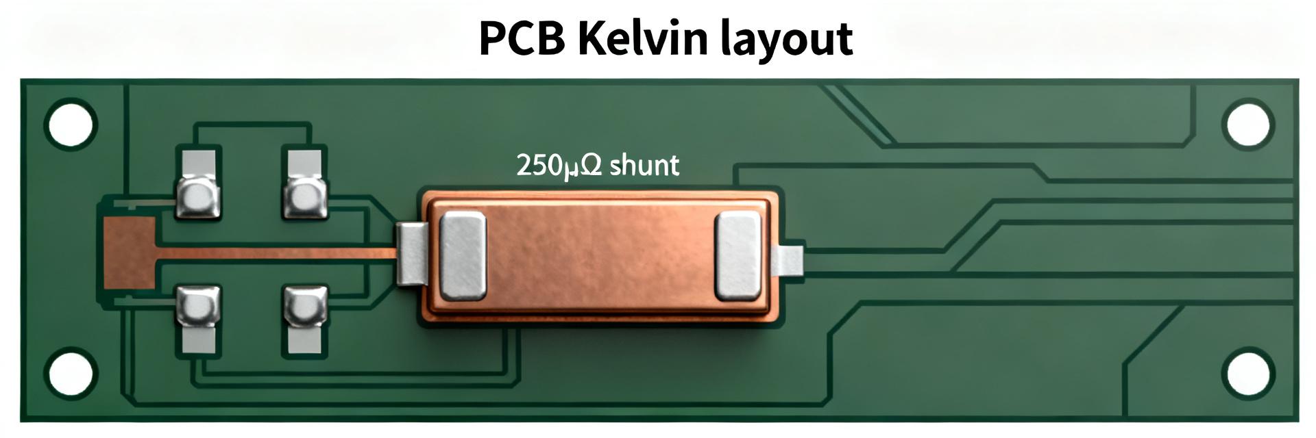
Mechanical Package & Dimension Callouts
Start by transcribing the package name, code, and the 2D dimension table from the official datasheet into a single reference drawing. Capture body length/width, overall height, lead/terminal pitch, and exposed-pad outline. Note tolerances for each dimension and add tolerance handling (± values) to pad design so manufacturing variability does not cause misalignment during pick-and-place and reflow.
Pinout & Functional Grouping
Map pin numbers to functions: power input, power output, ground, sense/feedback, and exposed thermal pad. Produce a simple pinout table for the footprint library showing pin number, net name, and function. Flag high-current pins and the exposed pad as requiring wider copper, thermal vias, and short return paths — these demand special layout attention early in the CAD flow.
Electrical & Thermal Specs Analysis
Thermal Performance Visualization
Estimated Junction Temp (ΔT) based on Pd:
Pull RθJA and RθJC, maximum junction temperature, and any thermal impedance curves from the datasheet. Use Pd × RθJA to estimate ΔT above ambient and plan a PCB strategy: exposed-pad area, thermal via count and placement, and copper pour connectivity. Recommend via sizes, via counts, and placement grid to meet the calculated ΔT for expected ambient and power dissipation.
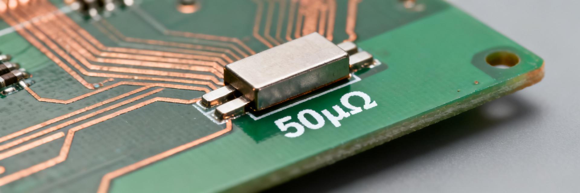
PCB Footprint & Land Pattern
Recommended Land Pattern from Datasheet
Convert 2D dimensions to SMD pad sizes by mapping body-to-pad clearances, terminal length, and lead pitch. Define SMD pad length and width to accommodate fillet formation and pick-and-place tolerances. Add soldermask clearance and a courtyard at recommended distances. Keep the land pattern adaptable to ± tolerance by designing pads slightly larger within assembly constraints to improve yield.
Example Footprint Case Study & Common Pitfalls
Workflow: Datasheet to CAD
- Import: Load datasheet 2D drawings as a background layer.
- Geometry: Create padstack for terminals and the central thermal pad.
- Expansions: Assign precise soldermask and paste mask layers.
- Thermal: Place the calculated thermal via grid (e.g., 3x3 or 4x4).
- Validation: Run DRC and verify against the 3D STEP model.
Top 6 Assembly Mistakes
- ❌ Incorrect pad-to-pad spacing
- ❌ Omitted thermal vias in high-power zones
- ❌ Insufficient soldermask expansion
- ❌ Ignored tolerance stack-up during layout
- ❌ Wrong paste coverage (too much/too little)
- ❌ Silkscreen printed over component pads
Final Design Checklist & Handoff
Pre-production Checklist
- Verified land pattern dimensions
- Thermal via count vs. Pd requirement
- BOM pad compatibility check
- 3D model clearance (Z-height)
- Orientation and inspection markers
Deliverables for Manufacturing
- CAD Footprint & 2D Drawing
- Recommended paste stencil specification
- Thermal via drill chart
- Pick-and-place coordinates
- Internal sign-off flow document
Key Summary
- Capture ORNTA5-1T0 mechanical dimensions precisely: body size, pad pitch, and exposed-pad outline, and include tolerance handling in the padstack to prevent assembly misalignment.
- Translate datasheet electrical specs into PCB rules: calculate Pd, use RθJA for ΔT, and convert allowable current into trace width and copper weight using IPC guidance.
- Design the PCB footprint with correct paste coverage, thermal via grid, and soldermask clearances; verify with DRC, 3D fit, and a pick-and-place test before release.