תיעוב מעמיק של דף הנתונים MDP160310K0GD04: מפרטים מרכזיים ונתוני בדיקה
The official datasheet figures indicate this MDP160310K0GD04 resistor network provides a nominal 10 kΩ per element, ±2% tolerance, and a TCR on the order of ±100 ppm/°C with a per‑element power rating appropriate for compact DIP arrays. This article extracts the most relevant numbers from the MDP160310K0GD04 datasheet, interprets test tables and curves, and delivers a practical bench and production validation plan engineers can apply directly to PCB designs and QA procedures.
1 — Component background & datasheet scope (background introduction)
1.1 Part identity, package, and variants
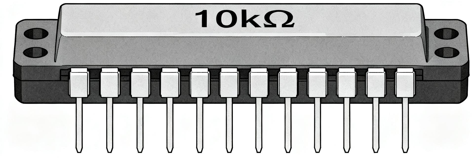
Part marking decodes as an MDP series 16‑pin dual‑in‑line resistor network with ten‑kilohm elements in an isolated element configuration. Package is standard 16‑pin DIP with body dimensions and seated height listed in the official datasheet; verify footprint pad spacing (2.54 mm pitch), body length and width, and pin‑to‑pin mapping against your PCB CAD models. Action: compare datasheet mechanical table to your footprint and log any tolerance discrepancies before layout freeze.
1.2 Intended applications and typical use cases
The datasheet positions the network for pull‑ups/pull‑downs, divider banks, and moderate power termination functions in space‑limited DIP circuits. It is well suited where multiple matched resistors are needed with small PCB area. Not recommended for high‑power discrete dissipation or high‑voltage isolation applications beyond the listed voltage rating. Action: match design power and voltage needs to datasheet limits; choose alternate packages for high‑power needs.
2 — Key electrical and thermal specs from the MDP160310K0GD04 datasheet (data analysis)
2.1 Electrical characteristics to extract and emphasize
Key electrical specs from the official datasheet to capture in your procurement and design notes include: nominal resistance 10 kΩ, tolerance ±2%, TCR ±100 ppm/°C, typical power per element (see datasheet power rating), maximum working voltage and element configuration (isolated elements). These values are usually specified at +25°C and with particular mounting conditions; record those test conditions alongside each value in your parts database. Action: copy the exact datasheet numbers and test conditions into BOM notes.
| Spec | Datasheet value | Notes / test conditions |
|---|---|---|
| Nominal resistance | 10 kΩ | ±2% tolerance at +25°C |
| Tolerance | ±2% | Measured DC, +25°C |
| TCR | ±100 ppm/°C | Over specified temperature range |
| Power per element | Refer to datasheet rating | Derate above specified temp; see curve |
| Voltage rating | Refer to datasheet | Maximum working voltage per element |
2.2 Thermal ratings and derating behavior
The datasheet provides a power‑derating curve that reduces allowable dissipation as ambient temperature rises. Note the maximum operating temperature and the slope of the derating line; if thermal resistance is listed, use it to predict temperature rise for a given load. Action: derate power to the specified percentage at your operating ambient and add margin—e.g., target 70–80% of rated power at higher ambient to preserve reliability.
| Ambient (°C) | Allowed power per element (% of rated) |
|---|---|
| 25 | 100% |
| 70 | 60–70% |
| 125 | 0% |
3 — Test data interpretation & practical measurements (data analysis / test data)
3.1 How to read and verify the datasheet test tables
Datasheet tables commonly show typical and maximum values with explicit test conditions; typical columns indicate nominal behavior, while max/min columns are guaranteed limits under stated conditions. Interpret Veff and ppm/°C values as conditioned by the measurement method in the notes. Action: when citing a value in design documentation, note whether it is typical or guaranteed and include the datasheet test condition footnote.
3.2 Recommended bench tests and expected results (test data)
Repeatable tests: DC resistance at +25°C (4‑wire if high accuracy), TCR across two or more temperatures, stepwise power dissipation to validate derating, voltage coefficient of resistance, and thermal imaging under steady load. For each test list equipment, procedures and pass/fail limits based on datasheet ± tolerance plus a small guard band (e.g., ±1% extra). Action: implement these tests on incoming lots and record mean and sigma against datasheet specs.
| Test | Equipment | Pass threshold | Notes |
|---|---|---|---|
| DC R @25°C | 4‑wire DMM | 10 kΩ ±2.2% | Allow small guard band |
| TCR | Temperature chamber, DMM | ±120 ppm/°C | Measured across specified range |
| Power soak | Programmable load, thermal camera | No thermal runaway, ΔR within spec | Monitor drift after soak |
4 — Application & design considerations (method/guideline)
4.1 Circuit-level tips: placement, noise, and parasitics
Place the network to minimize lead lengths to the node it serves; routing that crosses sensitive analog traces can introduce crosstalk. For precision dividers, separate elements used as different legs and avoid sharing copper islands that create thermal coupling. Action: route each critical resistor back to its node with short traces, add guard copper for thermal dissipation, and run a layout review focusing on parasitic resistance and coupling.
4.2 Thermal management and reliability best practices
Use additional PCB copper beneath and around the package for heat spreading; follow datasheet recommendations for clearance. For soldering, prefer profiles that match the datasheet thermal limits (reflow over wave if specified). Action: include a thermal qualification checklist—power soak at rated load for X hours, monitor resistance drift to validate long‑term behavior.
5 — Validation checklist & recommended test plan for production (action/advice / case-type)
5.1 Pre-production validation checklist
- Visual and dimensional inspection against datasheet mechanical table.
- Sample DC resistance measurement at +25°C (4‑wire preferred).
- Batch TCR spot checks across specified temp range.
- Power soak test on representative samples, monitor ΔR and temperature rise.
- Documented pass/fail results and disposition criteria.
5.2 Production test flow and reporting guidelines
Recommended flow: incoming inspection → sample electrical testing → burn‑in/power soak on statistical sample → lot acceptance per defined limits. Report mean R, standard deviation, and fail rate; use pass limits that are datasheet tolerance plus a guard band. Action: store results in a searchable QA database and trigger supplier review if fail rate exceeds thresholds.
Summary (10–15% of article)
Recap: the official datasheet lists 10 kΩ nominal elements in a 16‑pin DIP with ±2% tolerance and a TCR around ±100 ppm/°C; pay close attention to the per‑element power rating and derating curve when assigning loads. The top tests to run are DC resistance at +25°C, TCR across your operating range, stepwise power soak, and thermal imaging under load. Apply layout rules to minimize thermal and electrical coupling for precision applications.
- Key numbers to record: 10 kΩ nominal, ±2% tolerance, ±100 ppm/°C TCR, power per element and voltage rating from the official datasheet; use these in BOM notes and QA specs.
- Top tests: DC R @25°C, TCR sweep, power derating validation, and voltage coefficient check; each test should include pass limits derived from datasheet plus guard band.
- Design rules: short traces, dedicated copper for heat spreading, avoid shared islands to reduce thermal coupling in precision dividers.
FAQ
1 — How should I verify values in the MDP160310K0GD04 datasheet?
Verify by repeating key datasheet measurements on representative samples: DC resistance at +25°C with a 4‑wire method, TCR over the specified temp range in a chamber, and a power soak at rated dissipation using thermal imaging. Compare means and distributions to datasheet limits and apply a small guard band for production acceptance.
2 — What pass/fail margins are recommended versus the MDP160310K0GD04 datasheet specs?
Use the datasheet guaranteed limits as the baseline, then add a conservative guard band—commonly ±0.2–0.5% for low‑ohmic precision parts or an extra 10–20% on TCR and power derating thresholds depending on end‑use criticality. Define these margins in your QA plan and apply them consistently across lots.
3 — Which bench tests best expose thermal derating for MDP160310K0GD04?
Perform a stepwise power soak: increment power in defined steps to the element rating while recording steady‑state temperature via thermal camera and resistance drift. Plot allowed power vs. ambient to confirm the datasheet derating curve and validate your PCB copper spreading assumptions under realistic load conditions.
4 — What layout safeguards prevent crosstalk and thermal imbalance in MDP160310K0GD04 networks?
To prevent crosstalk and imbalance, route isolated elements with direct, short traces, avoid co-locating precision divider arms on shared inner thermal planes, and introduce dedicated copper pour under the package to spread heat across ambient dissipation limits.