FF200R12W2T7EB11BPSA1 Specs: Key Electrical & Thermal Data
The FF200R12W2T7EB11BPSA1 isn't just another IGBT module; it’s a 1200V, 200A powerhouse designed for high-efficiency industrial applications. But do you know its true thermal limits and electrical performance under stress? With power dissipation capped at 20 mW and an operating range spanning -40°C to +175°C, this EasyDUAL™ 2B component demands precise design integration. This guide breaks down the critical electrical data and thermal data you need to optimize your motor drives or auxiliary inverters.
Core Electrical Characteristics of the FF200R12W2T7EB11BPSA1
Voltage and Current Ratings Explained
You must understand that the collector-emitter voltage ($V_{CES}$) is rated at 1200 V, providing a robust safety margin for typical 480 VAC three-phase systems. The nominal current ($I_{C nom}$) stands at 200 A, while the peak repetitive current ($I_{CRM}$) reaches 400 A. These ratings define the module's capability in common emitter topology. When designing your circuit layout, ensure trace widths accommodate these peaks without excessive heating. The topology simplifies drive logic but requires careful attention to isolation barriers to prevent short circuits during switching transients.
Switching Performance Metrics
Low saturation voltage ($V_{CE,sat}$) is crucial for efficiency. Across various junction temperatures ($T_{vj}$), maintaining low $V_{CE,sat}$ reduces conduction losses significantly. Typical gate threshold voltages are standardized, ensuring compatibility with most driver ICs. Switching times are optimized for hard-switching topologies, directly impacting system efficiency in servo drives. Faster switching reduces turn-on/turn-off losses but may increase electromagnetic interference (EMI). You should balance speed against noise requirements by adjusting gate resistance values appropriately.
Critical Thermal Data and Management Requirements
Junction Temperature Limits and Derating Curves
The maximum operating temperature is +175°C, while the minimum is -40°C. Exceeding these limits risks permanent damage. Overload operation up to 175°C is possible but strictly time-limited. Interpreting derating curves is essential for continuous current ratings. As ambient temperature rises, the allowable current decreases linearly. You must calculate the thermal resistance from junction to case ($R_{thJC}$) to predict actual $T_{vj}$ under load. Ignoring derating leads to premature failure in high-temperature environments.
Power Dissipation and Heat Sink Integration
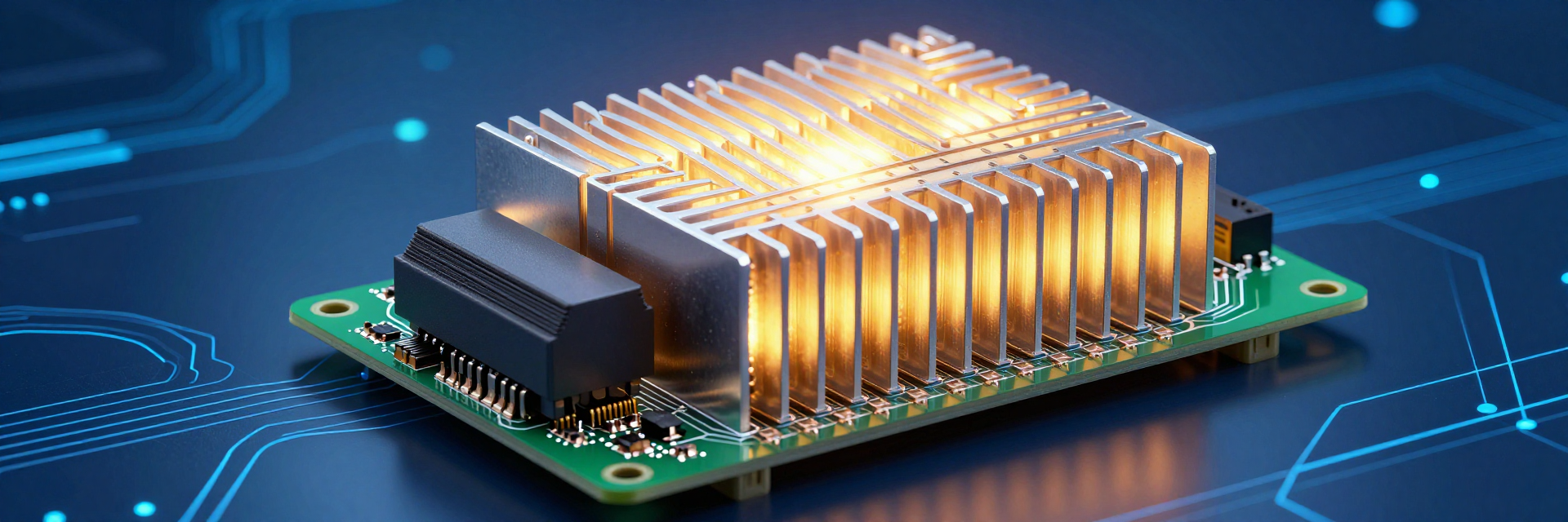
While static power dissipation specs like 20 mW refer to leakage or control pins, total device dissipation depends on switching and conduction losses. Proper heat sink integration is vital. Press-fit mounting styles offer reliable mechanical connections but require precise hole alignment to minimize contact resistance. Poor thermal interface materials can create hotspots. Ensure adequate airflow or liquid cooling to maintain $T_{vj}$ within safe limits. Thermal simulation tools help validate your cooling solution before prototyping.
| Parameter | Symbol | Value | Unit |
|---|---|---|---|
| Collector-Emitter Voltage | $V_{CES}$ | 1200 | V |
| Nominal Current | $I_{C nom}$ | 200 | A |
| Peak Repetitive Current | $I_{CRM}$ | 400 | A |
| Max Junction Temp | $T_{vj max}$ | 175 | °C |
| Min Operating Temp | $T_{vj min}$ | -40 | °C |
Practical Design Considerations for US Engineers
Application Suitability and Use Cases
This module excels in motor drives, air conditioning compressors, and auxiliary inverters. Compared to similar modules like the FS75R12W2T7, the FF200R12W2T7EB11BPSA1 offers higher current capacity, making it suitable for heavier loads. Supply chain planning is critical; standard lead times can extend to 19 weeks. Early procurement prevents project delays. Evaluate whether the extra headroom justifies the cost difference over smaller variants for your specific application needs.
Common Pitfalls in FF200R12W2T7EB11BPSA1 Implementation
Avoid exceeding $I_{CRM}$ without sufficient thermal headroom, as this causes immediate degradation. PCB layout must minimize parasitic inductance to prevent voltage spikes during switching. Long gate loops introduce noise and slow switching. Verify gate drive compatibility carefully; mismatched impedance leads to oscillation. Always double-check pinout diagrams against the datasheet to avoid catastrophic wiring errors during assembly.
Key Takeaways
- Understand that FF200R12W2T7EB11BPSA1 specs include a 1200V rating and 200A nominal current for robust industrial use.
- Monitor thermal data closely, ensuring junction temperatures stay below 175°C through proper heat sink integration.
- Analyze electrical data such as low $V_{CE,sat}$ to maximize efficiency in servo drives and inverters.
- Plan for long lead times and verify gate drive compatibility to avoid common implementation pitfalls.
Frequently Asked Questions
What is the maximum junction temperature for the FF200R12W2T7EB11BPSA1?
The maximum operating junction temperature ($T_{vj}$) is +175°C. Operating above this limit risks irreversible damage to the silicon chip. Engineers must design cooling systems that keep the junction well below this threshold under all expected load conditions, including transient peaks.
How does the FF200R12W2T7EB11BPSA1 compare to other IGBT modules?
It offers a balanced combination of 1200V blocking capability and 200A continuous current. Unlike lower-current modules, it handles higher loads without paralleling multiple devices, reducing board space and complexity. Its EasyDUAL™ package simplifies mounting compared to older screw-terminal designs.
Why is thermal derating important for this module?
Thermal derating ensures reliability by limiting current as temperature rises. Without it, the module could exceed safe junction temperatures, leading to failure. You must consult the derating curve in the datasheet to determine the maximum continuous current allowed at specific case temperatures.
What are common pitfalls in implementing the FF200R12W2T7EB11BPSA1?
Avoid exceeding $I_{CRM}$ without sufficient thermal headroom, as this causes immediate degradation. PCB layout must minimize parasitic inductance to prevent voltage spikes during switching. Long gate loops introduce noise and slow switching. Verify gate drive compatibility carefully; mismatched impedance leads to oscillation. Always double-check pinout diagrams against the datasheet to avoid catastrophic wiring errors during assembly.