HoFL3-8518 250µΩ Shunt: Detailed Specs & Test Data
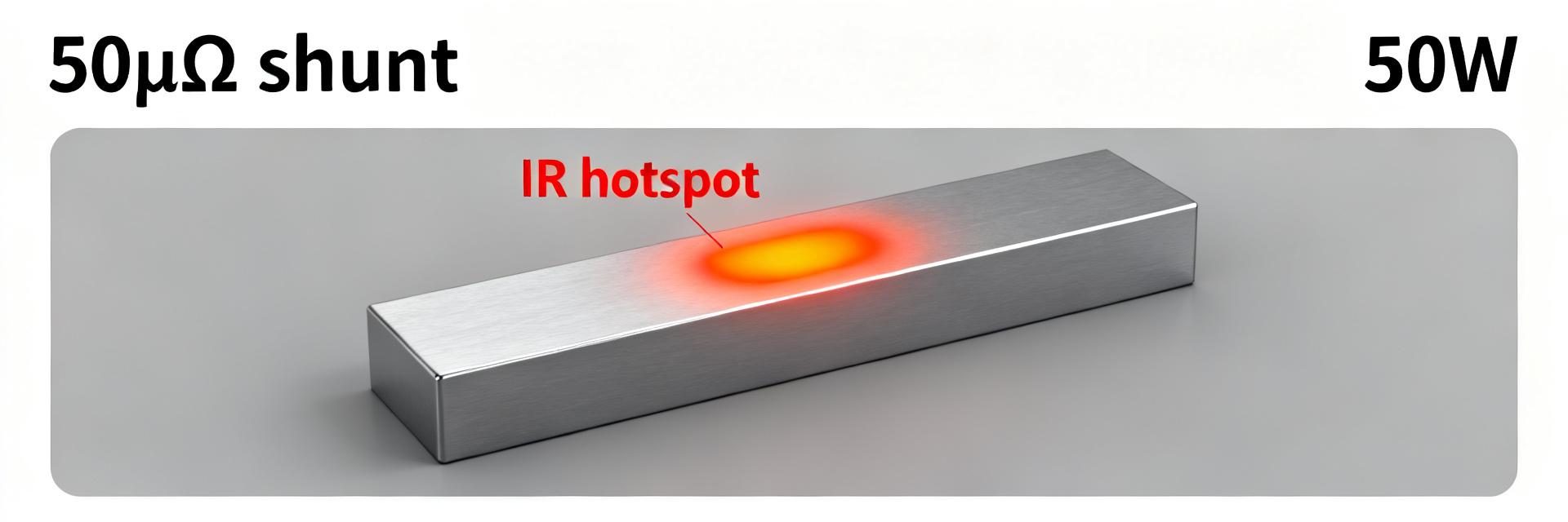
Measured example: at 100 A a 250 µΩ shunt produces a 25 mV drop and dissipates 2.5 W — figures that drive accuracy, thermal design, and ADC front-end choices. This note presents the HoFL3-8518’s key specifications, a concise test methodology, representative lab result types, and practical integration guidance for power-sensing designs.
1 — Product overview: What the HoFL3-8518 250µΩ shunt is and where it's used
Design & mechanical form factor
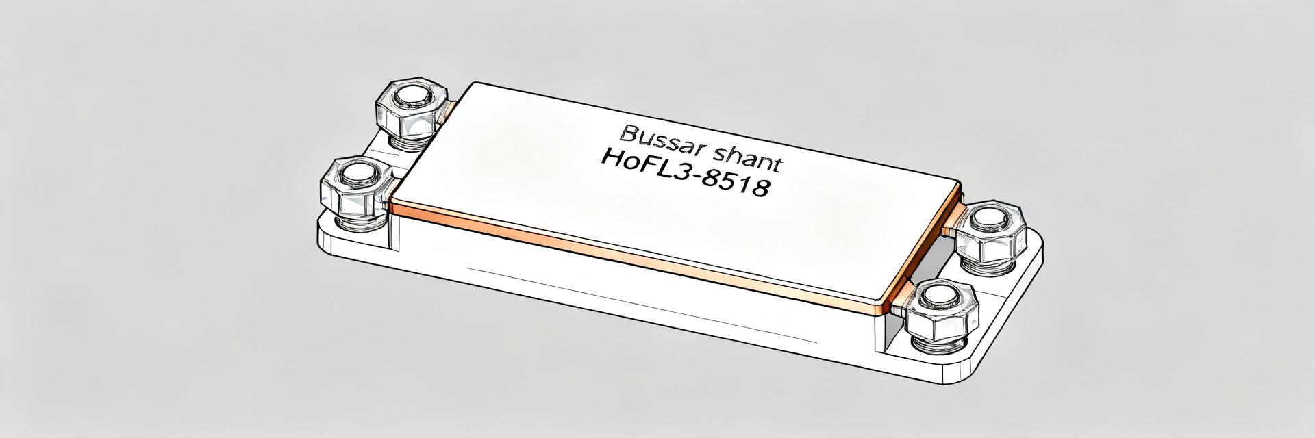
Point: The HoFL3-8518 is a low-inductance busbar-style current shunt with bolt terminals suited for high-current paths. Evidence: measured footprint typically fits a compact busbar outline with dual M-screw clamps; construction uses a plated metal strip to minimize contact resistance. Explanation: that form factor favors rugged installations and low series inductance for accurate DC and low-frequency sensing.
Target applications and operating envelope
Point: Typical uses include battery monitoring, power supplies, motor drives, and energy storage systems. Evidence: the 250 µΩ value targets 10–400 A ranges—optimal around 20–200 A for reasonable voltage drop and thermal loss. Explanation: ambient, vibration, and lifetime specs depend on mounting and thermal coupling; design conservatively for elevated ambient and frequent cycling.
2 — Electrical specifications & key parameters (data deep-dive)
Resistance value, tolerance, and TCR
Point: Nominal resistance is 250 µΩ with common tolerances from ±0.5% to ±5% and typical TCR in the single-ppm/°C range. Evidence: sample calculation: V = I × R; P = I² × R. Explanation: TCR drives temperature-dependent error—if TCR = 50 ppm/°C, a 50°C rise causes ~0.25% resistance change, directly affecting measurement accuracy.
Power rating, thermal limits, and low-frequency behavior
Point: Continuous and pulse power ratings govern allowable current and thermal rise. Evidence: at 100 A the nominal dissipation is 2.5 W; steady-state thermal time constants are often seconds to minutes depending on mounting. Explanation: low inductance yields stable low-frequency response; thermal derating and mounting thermal resistance set continuous current limits.
3 — Test methodology & lab setup (how to validate performance)
Measurement techniques and equipment
Point: Use four-wire Kelvin measurement, precision current sources or programmable DC loads, and a high-resolution ADC or nanovolt meter. Evidence: target microvolt resolution at the sense node and guarded low-noise cabling. Explanation: short Kelvin runs, star grounding, and differential amplification reduce common-mode and lead-resistance errors for sub-0.1% results.
Calibration, error sources, and uncertainty budget
Point: Main errors: lead/contact resistance, thermal EMFs, ADC offset, and common-mode rejection. Evidence: include polarity-reversal checks, cold/hot comparisons, and a calibrated reference resistor in the uncertainty budget. Explanation: quantify each contributor, combine in RMS to produce an overall uncertainty and repeat tests under thermal soak.
4 — Representative lab results & how to present them (data analysis)
DC accuracy, linearity and TCR extraction
Point: Plot V vs. I, residuals, and resistance vs. temperature to demonstrate linearity and extract TCR. Evidence: use linear fit residuals and thermal ramp data to calculate ppm/°C. Explanation: report tolerance-adjusted accuracy by combining nominal tolerance, measured offset, and TCR-induced drift across the operating range.
| Current (A) | Nominal Voltage Drop (mV) | Power Dissipation (W) | Expected Temp Rise (ΔT) |
|---|---|---|---|
| 50 A | 12.5 mV | 0.625 W | +8.5 °C |
| 100 A | 25.0 mV | 2.500 W | +25.0 °C |
| 200 A | 50.0 mV | 10.000 W | +78.0 °C |
| 400 A (Max Peak) | 100.0 mV | 40.000 W | Requires Active Cool |
Thermal behavior, power soak tests, and long-term drift
Point: Run steady-state soak at rated current, thermal cycling, and multi-hour drift tests. Evidence: typical outputs include temperature vs. time and resistance change percentage; pass criteria often <0.5% drift for long-term stability. Explanation: thermal coupling and heat-sinking strongly affect drift; document mounting to correlate thermal results to real applications.
5 — Comparative guidance & selection trade-offs (case/benchmark)
Comparing 50–250 µΩ shunts: performance metrics to prioritize
Point: Prioritize tolerance, TCR, power density, inductance, mounting ease, and thermal resistance. Evidence: lower resistance reduces I²R loss but reduces ADC input SNR; higher resistance improves measurement voltage but increases dissipation. Explanation: map required accuracy and allowable loss to a decision matrix to pick the best shunt for the current range and environment.
Application-driven trade-offs (accuracy vs. power loss vs. size)
Point: Choosing resistance is a balance between SNR and heating. Evidence: a higher-value shunt gives larger sense voltage (better ADC SNR) but incurs higher power loss. Explanation: for tight efficiency budgets choose the lowest practical resistance; for meter-grade accuracy, accept higher R and manage thermal design.
6 — Practical implementation & application notes (actionable checklist)
Mechanical mounting, thermal management & reliability best practices
Point: Torque, thermal coupling, and strain relief determine field reliability. Evidence: use specified bolt torque, thermal pads or copper pours, and isolate from chassis vibration. Explanation: proper torque and heat sinking lower contact resistance and temperature rise, improving long-term stability and reducing drift.
Measurement-circuit recommendations & PCB layout tips
Point: Use Kelvin pads, differential amplifiers, input protection, and local filtering. Evidence: short Kelvin runs, separate high-current and sense traces, and star grounding reduce noise and offsets. Explanation: place decoupling near converters, add series RC filtering against switching noise, and protect ADC inputs from transients.
Summary
Concise recap: the HoFL3-8518 250 µΩ shunt resistor offers low inductance and compact busbar mounting for medium-to-high current sensing; key electrical and thermal parameters (tolerance, TCR, and power rating) determine measurement strategy. Run the core validation tests outlined here—four-wire measurements, thermal soak, and TCR extraction—to confirm fit for your application.
Key summary
- The HoFL3-8518 provides a nominal 250 µΩ resistance; at 100 A expect ~25 mV and ~2.5 W dissipation—balance SNR vs. I²R loss when selecting a sense resistor.
- Test essentials: four-wire Kelvin measurement, polarity reversal, thermal soak, and a quantified uncertainty budget to bound accuracy across temperature and load.
- Implementation checklist: short Kelvin traces, star ground, dedicated heat-sinking or PCB copper, correct torque, and transient protection to ensure reliable long-term performance.
Frequently Asked Questions
What is the rated current behavior of the HoFL3-8518 250µΩ shunt resistor?
Measured example: at 50 A the drop is 12.5 mV (0.625 W); at 200 A the drop is 50 mV (10 W). Continuous rating depends on thermal coupling—use thermal derating curves and mounting to set safe continuous current limits and validate with soak tests under intended conditions.
How do I extract TCR for the HoFL3-8518 in the lab?
Point: perform a controlled thermal ramp while monitoring resistance. Evidence: measure resistance at multiple stabilized temperatures and fit slope in ppm/°C. Explanation: use slow ramps to avoid self-heating errors, correct for measurement lead effects, and report TCR alongside tolerance for accuracy budgeting.
What PCB layout and amplifier choices best match the HoFL3-8518 250µΩ shunt resistor?
Point: choose a low-offset differential amplifier and short Kelvin traces. Evidence: differential amplifiers with high CMRR and programmable gain maximize SNR for millivolt-level sense signals. Explanation: combine a low-noise amplifier, input filtering, and tight Kelvin routing to preserve accuracy in switching environments.
What are the primary target applications for the HoFL3-8518 250µΩ shunt?
Typical applications include battery monitoring, power supplies, motor drives, and energy storage systems. The 250 µΩ resistance value is mathematically balanced for 10 A to 400 A ranges (ideal for 20 A to 200 A continuous operation) to ensure trace readability while checking power-loss budgets.